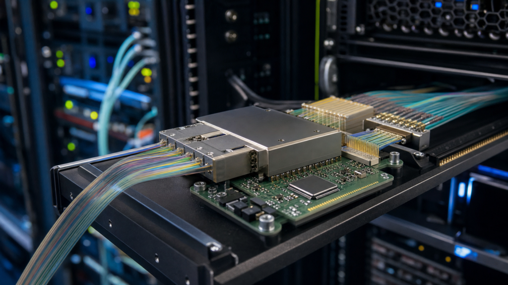
Optical circuit switches are again a serious datacenter architecture topic, and Google's Apollo paper is the clean public proof point: it describes a large-scale production OCS deployment and says its datacenter requirements drove an internally developed 3D MEMS-based OCS. For MEMS mirror driver ICs, that shifts the analog question away from generic "high voltage DAC" selection and toward a set-and-settle problem: voltage range, output current, settling behavior, drift, load capacitance, and lifecycle risk all matter together.
ADI's public product pages show a lifecycle transition across its 32-channel high-voltage DAC driver family: AD5535 is obsolete, AD5535B is not recommended for new designs, and AD45335 is recommended for new designs. The AD5535B-to-AD45335 comparison changes drive current and falling-edge settling enough that OCS engineers should validate against the actual mirror load and reconfiguration budget before assuming the newer part is a drop-in design answer.
Why Now
OCS is no longer only a lab concept for datacenter fabrics. Google's Apollo paper describes what the authors call a large-scale production deployment of optical circuit switches for datacenter networking. It also states that datacenter OCS requirements such as cost, port count, switching time, and optical performance drove the design choices for an internally developed 3D MEMS-based OCS.
AI infrastructure adds a second reason to watch this area. Recent public research such as InfinitePOD frames large language model training as a high-bandwidth-domain problem and proposes optical circuit switching as one way to attack scale, cost, and fault-containment pressure. That paper is not a MEMS-mirror driver source, but it reinforces the system-level point: optical circuit switching is being pulled back into the datacenter architecture conversation.
This creates a concrete component question: what driver IC class do MEMS-based OCS mirrors actually require, and what does ADI's current 32-channel high-voltage DAC lifecycle imply for new OCS designs?
OCS Architecture Comparison
A useful comparison from recent OCS market commentary is that optical circuit switching should not be read as a one-for-one replacement for electronic packet switching. EPS remains the right layer for packet-level forwarding, buffering, queueing, telemetry, encryption, and rapidly changing traffic. OCS becomes attractive when the network can hold an optical circuit map long enough to amortize the reconfiguration event: AI training phases, upper-layer scale-out links with less packet manipulation, or large data movement across sites.
The Google TPU v4 paper supports that system framing. It says OCSes dynamically reconfigure TPU v4's interconnect topology to improve scale, availability, utilization, modularity, deployment, security, power, and performance. It also reports that OCSes and underlying optical components were less than 5% of TPU v4 system cost and less than 3% of system power.
For the driver IC, this distinction matters because the analog problem is not packet switching. The MEMS driver has to place the mirror array accurately at topology-change time, settle without violating the optical error budget, and then hold calibrated voltages with low enough drift until the next mapping change. That is why output current, falling-edge behavior, leakage, temperature drift, channel matching, board parasitics, and calibration hooks matter as much as the nominal high-voltage range.
MEMS Versus Other OCS Approaches
Not every OCS architecture creates the same driver-IC requirement. Semi Fundamental's March 2026 OCS overview groups the field into MEMS, LCoS, waveguide, and piezoelectric approaches. For this article, the important point is how the optical steering mechanism changes the electronics problem.
| OCS approach | Optical steering method | Main advantage | Main constraint | Driver-IC implication |
|---|---|---|---|---|
| MEMS OCS | Movable micromirrors steer light paths | Mature near-term route for datacenter OCS; millisecond-class reconfiguration and relatively low insertion loss are attractive for AI training fabrics | Mechanical lifetime, calibration, mirror control, and port-count scaling | Closest fit to the AD5535B/AD45335 class: many high-voltage, low-leakage, quasi-static mirror-control channels |
| LCoS OCS | Liquid crystal on silicon changes the optical path through voltage-controlled phase/polarization behavior | Potentially longer operating life because it avoids a large moving mirror array | Slower reconfiguration and tighter polarization/optical alignment complexity | Still voltage-controlled, but the load and driver architecture are not the same as electrostatic MEMS mirror deflection |
| Waveguide OCS | Integrated photonic waveguides, MZIs, or ring resonators route light on chip | Potential for microsecond-class switching and more dynamic topology changes | Insertion loss, crosstalk, amplifier integration, and port-count scaling | Moves the driver problem toward high-speed photonic control rather than quasi-static 50-200 V MEMS mirror DACs |
| Piezoelectric OCS | Piezo actuators physically align optical paths | Very low insertion-loss potential | Cost, actuator mechanics, and manufacturing complexity | Requires an actuator-driver design, not a drop-in MEMS HV DAC assumption |
This comparison narrows the claim of the article. AD5535B and AD45335 are relevant to MEMS mirror deflection/control and optical crosspoint switching; they should not be treated as universal OCS driver answers for LCoS, waveguide, or piezoelectric architectures.
Port Scaling Turns the Driver Into a System Problem
The same OCS overview frames recent commercial systems around 128×128 and 144×144 configurations, with newer 300×300-class systems derived from larger 384×384 platforms and future work pushing beyond that. Treat those numbers as market context, not as a component specification. The driver-IC takeaway is more general: port-count scaling multiplies analog channels, calibration points, and failure opportunities.
A 32-channel high-voltage DAC is only one tile in a larger mirror-control plane. As OCS radix rises, system architects have to manage output settling skew across many channels, leakage over long hold intervals, channel-to-channel accuracy, board parasitics, production trim, field recalibration, and fault isolation. At high port counts, the driver IC is no longer just a voltage-output component; it becomes part of the switch's optical alignment, test, and serviceability strategy.
The Quasi-Static Distinction
Here, "quasi-static" is a driver-level framing, not a universal claim that every OCS platform has the same timing requirement. A MEMS optical circuit switch establishes an optical path and keeps it in service until the next reconfiguration event. Google's Apollo paper evaluates datacenter OCS design around switching time and optical performance, while ADI positions the AD5535/AD5535B/AD45335 class for optical MEMS mirror deflection/control and optical crosspoint switches.
Taken together, those public facts point to a set-and-hold analog problem: move the mirror to a target angle, settle within the optical error budget, and keep the voltage stable enough while the circuit remains active. That is different from scanning MEMS applications, where the mirror continuously oscillates and the driver is optimized around repetitive dynamic motion.
The exact settling window, acceptable angular error, and hold duration are system-specific. They should come from the OCS architecture and MEMS mirror load, not from a generic DAC headline spec.
The Incumbent Benchmark Landscape
ADI's 32-channel high-voltage DAC family is the public reference point for this driver class. Three parts define the current landscape:
- AD5535: Discontinued. (ADI product page)
- AD5535B: Not recommended for new designs. (ADI product page)
- AD45335: Recommended for new designs. Preliminary datasheet Rev. B, 2024-10-21. (ADI product page)
All three share a common specification baseline: 32 channels, 14-bit DAC resolution, 50-200 V programmable full-scale via REF_IN, 3-wire SPI up to 30 MHz, an integrated temperature diode, a 15 x 15 mm CSP_BGA 124-ball package, a 200 pF capacitive load test condition, and a 1.2 MHz channel update rate. (ADI AD5535B datasheet; ADI AD45335 preliminary datasheet Rev. B)
Drive current and settling diverge:
| Parameter | AD5535B | AD45335 |
|---|---|---|
| Source current | 550 uA | 150 uA |
| Sink current | 2.8 mA | 40 uA |
| Settling, 200 pF, large step | 60 us | 190 us rising / 470 us falling |
| Slew rate, 200 pF | 3 V/us | 0.2 V/us falling |
(ADI AD5535B datasheet; ADI AD45335 preliminary datasheet Rev. B)
ADI lists AD45335 as recommended for new designs. The datasheets include no statement that AD45335 is an official replacement for AD5535B, and that assumption should not be carried into a new design without verification.
What the Drive Current Delta Actually Means
The most significant difference at the 200 pF datasheet test condition is in sink current: AD5535B sinks 2.8 mA; AD45335 sinks 40 uA – a reduction of approximately 70x. This directly affects the falling-edge settling timeline.
INFERENCE: Dividing 470 us by 60 us yields approximately 7.8x. Engineers evaluating this comparison at the 200 pF test condition may find that AD45335 falling-edge settling is roughly 8x slower than AD5535B under those specific conditions. This is a derived ratio from two datasheet numbers, not a characterized system measurement.
Whether this delta matters depends on the actual system:
- If the fabric-level reconfiguration budget is measured in milliseconds rather than microseconds, a few hundred microseconds of additional falling settling may fall within margin.
- If actual MEMS mirror capacitance plus board parasitics substantially exceeds 200 pF, the absolute settling times for both parts will increase, and 40 uA of available sink current may become a constraint that requires design attention.
- If the system requires successive mirror steps within a tight time window, the falling-edge behavior requires explicit bench characterization, not datasheet extrapolation.
Engineers may find that AD45335 meets their OCS settling requirement at their specific load and step pattern. They may also find that the lower sink current calls for a modified control strategy or supplementary passive discharge. Neither conclusion is available from the datasheet comparison alone.
What Engineers Should Do
- Establish actual load before selecting a driver. Measure or simulate mirror capacitance plus all PCB routing parasitics. The ADI 200 pF condition is a defined test point for comparison, not a system characterization. Load on a populated PCB with real MEMS mirrors may differ substantially.
- Define settle-time budget before interpreting specs. Determine what optical switching latency the fabric can tolerate, then work backward to the mirror-level angular error and timing requirement. A driver with 470 us falling settling is not automatically disqualifying if the system budget is 10 ms; it may be a serious constraint if the budget is 500 us.
- Characterize falling-edge behavior explicitly. In quasi-static OCS, mirror moves occur in both directions. Validate rising and falling settling at actual load, and verify what angular error is acceptable at the settle deadline. If passive or active discharge is needed to improve falling settling at low sink currents, design that into the board architecture before taping out.
- Do not assume package similarity implies pin compatibility. AD5535B and AD45335 share a package class. Check pinout, supply sequencing, and SPI timing independently before committing a layout. (ADI AD45335 preliminary datasheet Rev. B; ADI AD5535B datasheet)
- Track the AD45335 datasheet to final release. The document is marked preliminary as of Rev. B (2024-10-21). Specifications may change before production release. Build the final design against a released, non-preliminary document.
Caveats
- ADI's 200 pF test condition is defined for controlled comparison, not to represent any specific MEMS mirror load. Actual capacitance varies by device design, process geometry, and board parasitics.
- Drive current alone does not determine mirror settling. Control loop architecture, series resistance in routing, bypass capacitance, and mechanical damping all affect the angular settling trajectory.
- No published source in this review confirms that OCS MEMS mirrors universally settle within any specific time window; system timing requirements are platform-specific.
- AD45335 is listed as recommended for new designs. It has not been publicly confirmed as a qualified or validated component for MEMS OCS systems by ADI or any named OCS platform supplier.
- This article makes no claim that AD45335 is unsuitable for OCS. Suitability requires validation by the design engineer against their specific load, angular error budget, and settle-time requirement.
- The ~8x slower falling settling figure is an inference calculated from two datasheet numbers, not a characterized result from the same test setup.
- Semi Fundamental's OCS article is used here as secondary market/architecture commentary. Pricing, shipment, vendor-share, and roadmap details should not be treated as component qualification evidence.
Sources
- Ryohei Urata et al., "Mission Apollo: Landing Optical Circuit Switching at Datacenter Scale," arXiv:2208.10041, 2022. Used for datacenter-scale OCS deployment context and the public statement that Apollo used an internally developed 3D MEMS-based OCS: https://arxiv.org/abs/2208.10041
- Norman P. Jouppi et al., "TPU v4: An Optically Reconfigurable Supercomputer for Machine Learning with Hardware Support for Embeddings," arXiv:2304.01433, 2023. Used for Google TPU v4 system-level OCS context, including topology reconfiguration benefits and the reported OCS/optical component share of system cost and power: https://arxiv.org/abs/2304.01433
- Chenchen Shou et al., "InfinitePOD: Building Datacenter-Scale High-Bandwidth Domain for LLM with Optical Circuit Switching Transceivers," arXiv:2502.03885, 2025. Used only for current AI/LLM high-bandwidth-domain OCS context, not for MEMS mirror driver claims: https://arxiv.org/abs/2502.03885
- Semi Fundamental, "Optical Circuit Switches (OCS) Fundamentals," March 26, 2026. Used for secondary market/architecture comparison of OCS use cases, OCS-vs-EPS framing, port-count context, and MEMS/LCoS/waveguide/piezo OCS taxonomy, not for ADI driver-IC specifications: https://semifundamental.substack.com/p/optical-circuit-switches-ocs-fundamentals
- Analog Devices AD5535 product page. Used for product lifecycle, 32-channel/14-bit/50 V to 200 V description, optical MEMS mirror deflection/control positioning, and optical crosspoint switch application: https://www.analog.com/en/products/ad5535.html
- Analog Devices AD5535B product page. Used for product lifecycle, 32-channel/14-bit/50 V to 200 V description, optical MEMS mirror deflection/control positioning, optical crosspoint switch application, and AD45335 alternative-part lifecycle note: https://www.analog.com/en/products/ad5535b.html
- Analog Devices AD45335 product page. Used for product lifecycle, 32-channel/14-bit/50 V to 200 V description, 150/40 uA source/sink drive capability, optical MEMS and optical crosspoint switch applications, and preliminary Rev. B datasheet listing dated 2024-10-21: https://www.analog.com/en/products/ad45335.html
- Analog Devices AD5535B datasheet, Rev. B. Used for AD5535B detailed electrical comparison values.
- Analog Devices AD45335 preliminary datasheet, Rev. B, 2024-10-21. Used for AD45335 detailed electrical comparison values.