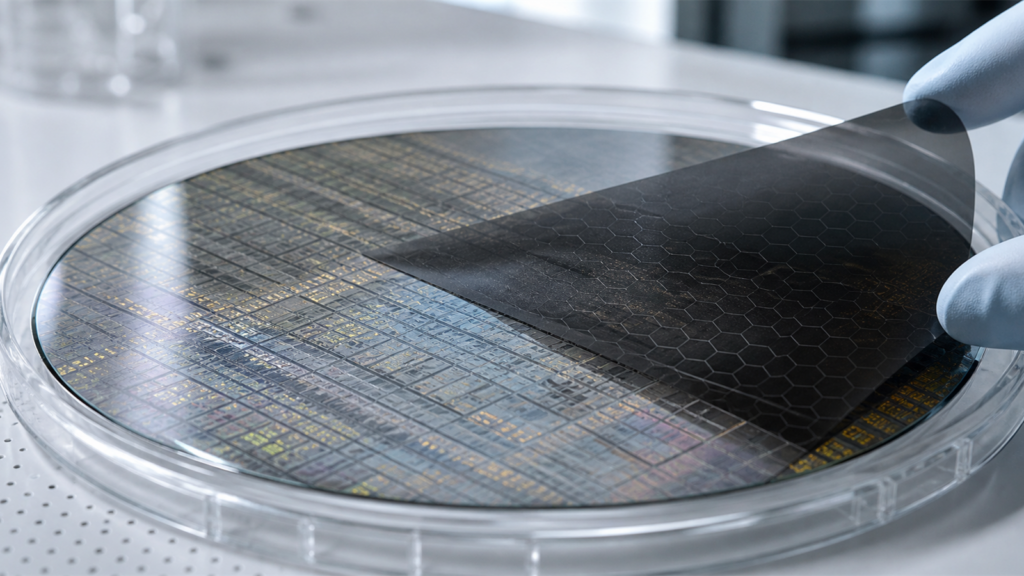
Graphene is one of the most over-cited materials in semiconductor presentations. A single atomic layer of carbon arranged in a honeycomb lattice does have extraordinary theoretical properties — thermal conductivity approaching 5,000 W/m·K in-plane, current density limits a thousand times higher than copper, electron mobility that shames silicon. Those numbers appear in every graphene pitch deck because they are real.
What the pitch decks usually omit is the word “theoretical,” and the qualifier “in a pristine suspended monolayer on a laboratory stage.” The graphene that ships in commercial quantities today is not that. Most commercial graphene products are reduced graphene oxide, graphene nanoplatelets, or pyrolytic graphite films. They are useful materials. They have different properties, different costs, and different competitive dynamics than monolayer CVD graphene. Conflating them is the beginning of every misguided project in this space.
The semiconductor industry has been here before. Carbon nanotubes were going to replace copper interconnects and silicon transistors. They are now used in battery electrodes and composite materials, where they are genuinely valuable. Graphene will follow a similar path — useful in specific, lower-integration-barrier applications long before it touches a wafer fab process.
The question for a semiconductor materials or components business is not “is graphene real?” The question is which applications have crossed from academic demonstration to something a customer will qualify, pay for, and put into production.
The Common Misunderstanding
The common misunderstanding is that “graphene in semiconductors” is a single conversation. It is not. It is at least five different conversations that require completely different technical arguments, timelines, and competitive analyses.
Graphene as a transistor channel material for logic — the application most often headlined — faces a fundamental materials physics problem that no engineering team has solved: graphene has no bandgap. A transistor without a bandgap cannot be switched off. The on/off current ratio for a standard graphene field-effect transistor is roughly 2 to 10. CMOS logic requires more than 10,000. This is not a problem of manufacturing quality or process maturity. It is a property of the hexagonal carbon lattice, and every approach to engineer around it — nanoribbons, twisted bilayers, chemical functionalisation — introduces a different fatal tradeoff. A 2024 Nature paper from Georgia Tech reported a semiconducting epitaxial graphene structure on silicon carbide achieving a 0.6 eV bandgap — materially larger than the roughly 0.26 eV typically cited for conventional epitaxial graphene on SiC — with high room-temperature carrier mobility; this is a meaningful materials-physics result, but no transistor on/off ratio has been published for this structure, and no foundry interest or production roadmap has been reported. A larger bandgap alone does not establish CMOS-adequate switching. No foundry has graphene logic on any production roadmap.
Graphene as a thermal management material is a different conversation entirely. Commercial rGO and graphene thermal films have been in consumer electronics production for years. Huawei smartphones have used graphene-based cooling films since the Mate series. The Sixth Element in Changzhou is a confirmed supplier. The supply chain exists. The performance is real. The question is not whether graphene thermal films work — it is whether a new entrant can compete with established Chinese manufacturers and move the application from consumer electronics into semiconductor packaging.
Treating these as the same conversation produces investments that are technically illiterate, market-entry strategies that are 10 years too early or 5 years too late, and customer conversations that will be ended quickly by anyone who knows the field.
What the Material Taxonomy Actually Means
Before any technical or commercial discussion, a clear terminology framework is necessary, because the word “graphene” is used commercially to cover materials that differ by orders of magnitude in cost, performance, and manufacturing process.
Monolayer CVD graphene is grown on copper foil by chemical vapour deposition and transferred to a target substrate. Its in-plane thermal conductivity in a transferred state is roughly 600 to 1,000 W/m·K. It costs between $1.50 and $10 per square centimetre in small quantities. It is used primarily in research on BEOL interconnects, diffusion barriers, sensors, and photonic devices. It is not a volume commercial material.
Reduced graphene oxide is made by oxidising graphite to graphene oxide and then chemically or thermally reducing it. In film form, practical in-plane thermal conductivity is 100 to 600 W/m·K. Industrial bulk pricing from Chinese producers is $5 to $50 per kilogram. This is the material in most commercial graphene thermal and EMI shielding products.
Pyrolytic graphite film is made by pyrolysing a polymer film at high temperature. In-plane thermal conductivity: 700 to 1,000 W/m·K. Panasonic PGS and Kaneka pyrolytic graphite are established products in consumer electronics thermal management. These are the direct competitive reference for any graphene thermal film supplier, not copper or thermal paste.
Every price, performance, and timeline claim in graphene should be checked against which of these materials is actually being discussed.
Where Graphene Has Crossed the Lab Boundary
Two applications have moved from laboratory to commercial production. One is niche. One is volume but China-dominated.
Paragraf, a Cambridge-based company, ships production graphene Hall effect sensors. Paragraf’s Hall sensors cover a range from cryogenic millikelvin temperatures to 700 K, span up to 30 T field strength across three product variants, survive radiation environments that degrade GaAs sensors, and have been independently tested at CERN’s Magnetic Measurement Laboratory; Paragraf’s large-area graphene growth process now reaches 8-inch wafer diameter. The commercial reality is genuine — but the market is specialised and small. This is not a high-volume semiconductor supply chain play.
Consumer electronics thermal films are volume. Multiple Chinese manufacturers including The Sixth Element, 2D Carbon Tech in Suzhou, Ningbo Morsh Technology, and Tianjin Kimwan Carbon Technology produce rGO and graphene composite thermal films that are incorporated into high-end smartphones and laptops. Huawei’s adoption is confirmed and public. The supply chain is operational. Korean producers including GALLOP INNOTEK and BestGraphene also supply this market.
These are the only two segments where a customer asking for graphene will receive a commercially qualified product in return. Everything else is being developed, investigated, patented, or piloted.
The BEOL Interconnect Research — What It Actually Shows
The most technically significant graphene work in the semiconductor supply chain is happening in back-end-of-line interconnect research, and it is important because it shows both how far graphene has come and how far it still has to go.
At sub-5 nanometre BEOL nodes, copper faces a problem it has never had before: resistivity rises sharply as wire width approaches the mean free path of electrons. Ruthenium, cobalt, and molybdenum are being evaluated as copper successors or supplements. Graphene is in that same research pipeline.
IMEC has published work on hybrid graphene-metal interconnects — graphene capping layers that reduce surface scattering in metal lines, and graphene-metal multilayer stacks — as candidates for extending the BEOL roadmap beyond 1 nanometre. Samsung and Seoul National University demonstrated in-situ CVD graphene grown as a diffusion barrier and copper nucleation layer inside interconnect trenches, replacing the TaN/Ta liner at near-zero thickness. A 2025 Nature Communications paper from Penn State reported a ruthenium-supported reduced graphene oxide barrier meeting lab performance targets for advanced nodes. A team at National Taiwan University published a direct experimental result in Nano Letters (2024) showing graphene-encapsulated cobalt interconnect wires — grown at 380°C, within BEOL thermal budget — with 27 percent lower resistance and 36 times longer electromigration lifetime than uncoated cobalt lines, verified in physical and electrical characterisation. In April 2026, ASX-listed Adisyn reported graphene deposition on a standard industrial ALD system, on a 1 cm × 1 cm coupon, below 450°C — notable for compatibility with industrial equipment, though the company’s own announcement states that film optimisation, repeatability testing, and scale-up to wafer formats all remain ahead, and no foundry partner has been named.
These are meaningful milestones. They are also laboratory demonstrations in research fabs, and the integration challenges that remain — wafer-scale CVD uniformity below the CMOS thermal budget, contact resistance at graphene-metal interfaces, adhesion to low-k dielectrics, and process qualification — are measured in years, not months. No foundry has announced production plans. The realistic timeline for graphene in BEOL production is a decade away at current rates of progress.
What Customers Actually Care About
A customer evaluating graphene materials for any semiconductor-adjacent application will move quickly from “what is graphene’s thermal conductivity?” to a sharper checklist:
- Which graphene material type is actually being proposed — monolayer CVD, few-layer CVD, rGO, graphene nanoplatelets, or pyrolytic graphite — and what are the measured properties of the specific product, not the theoretical properties of ideal graphene?
- What is the lot-to-lot consistency of the material: layer count distribution, oxygen content (for rGO), lateral flake size, purity, and absence of metal contamination?
- For thermal applications: what is the out-of-plane (cross-plane) thermal conductivity, which is the relevant metric for a die-attach TIM, not the in-plane value that appears in marketing?
- What JEDEC or industry-standard reliability data exists — HAST/uHAST, MSL/reflow cycling, thermal cycling, adhesion, delamination, ionic contamination, outgassing?
- What is the incumbent qualification status — has any named OSAT, packaging house, or module assembler qualified the product in production?
- What is the particle contamination, metal contamination, and outgassing profile for semiconductor-clean processing environments?
- What is the supply continuity model — can the supplier guarantee lot consistency and volume availability under a production purchase agreement?
- What is the actual system-level cost comparison versus incumbent solutions including Panasonic PGS, Kaneka pyrolytic graphite, Carbice CNT TIM, Henkel/Bergquist Phase Change, Parker/Chomerics THERMAGAP, and Momentive thermal pastes?
- For BEOL or process integration: is the deposition process CMOS-compatible below 400°C, and what is the pinhole density, adhesion, and via integration strategy?
- Who in the customer’s organisation owns the qualification decision, and what is their standard qualification timeline?
These are the questions that determine whether a graphene supplier gets a development agreement or a polite “we’ll monitor the space.”
The Practical Near-Term Insertion Points
Three application areas have the clearest path from current commercial reality to semiconductor-adjacent revenue, in descending order of near-term probability.
Graphene and rGO thermal films for package-adjacent thermal management have the strongest case. The rGO supply chain is operational. Consumer electronics deployment is confirmed. The move into power modules, RF modules, AI accelerator thermal stacks, and SSD thermal management requires module-level qualification — not front-end fab integration. The technical barriers are HAST/uHAST, MSL/reflow, and CTE compatibility, which are tractable in an 18 to 36 month development programme. The business challenge is competing with entrenched Chinese suppliers on cost and with Panasonic and Kaneka on reliability track record.
Graphene EMI shielding films for advanced electronics modules occupy a credible but narrower position. Commercial graphene EMI products exist for general electronics — Nanotech Energy, LayerOne, NanoEmi all supply them. The value proposition versus copper and aluminium shielding requires a clear answer: does graphene win on weight, on combined thermal and EMI functionality in a single film, or on ultra-thin form factor for high-density modules? Without a specific technical differentiation argument, the entry is speculative. Semiconductor package qualification adds a further validation step that has not yet been publicly completed by any graphene EMI supplier.
Anti-corrosion coatings for non-cleanroom fab infrastructure are realistic for external facility components — equipment cabinets, exhaust ducting, abatement hardware, wet-bench secondary structures — where salt-spray performance matters and semiconductor contamination requirements do not apply. For plasma-facing components or wafer-contact hardware, the contamination and outgassing qualification requirements add 2 to 4 years to any development timeline. This is a medium-term speculative entry, not a near-term one.
Where ChinaSemiOps Creates Practical Value
ChinaSemiOps can help customers navigate graphene claims by making the vocabulary and the timeline assumptions explicit before any procurement or development decision is made.
The first practical service is material classification. A supplier claiming “graphene TIM with 3,000 W/m·K thermal conductivity” is describing monolayer suspended graphene. A film product that can be purchased and installed describes an rGO or pyrolytic graphite product with 100 to 600 W/m·K in-plane conductivity and 5 to 10 W/m·K cross-plane. Helping a customer understand which number is relevant to their application — usually the cross-plane figure — eliminates immediately the gap between supplier claim and engineering reality.
The second service is supply chain mapping. Chinese graphene and rGO producers for thermal management applications are not well known outside China. The Sixth Element, 2D Carbon Tech, Morsh Technology, and Kimwan Carbon are the relevant producers for rGO thermal films — not the battery-additive graphene powder companies that appear in most market reports. Identifying which Chinese supplier actually serves the electronics thermal management market, with confirmed customer references, is actionable intelligence that is not readily available from public sources.
The third service is qualifier identification. For a customer moving from consumer electronics deployment to semiconductor module qualification, the specific additional requirements — JEDEC reliability package, particle and contamination characterisation, lot-consistency documentation — define the gap between “our material works in phones” and “our material is qualified for your SiP.” ChinaSemiOps can help suppliers and customers define that gap precisely, so that development agreements are scoped to close it rather than to generate inconclusive data.
- Classify the actual graphene material type and map claimed performance to measured performance
- Identify the correct Chinese and Korean thermal film suppliers for semiconductor-adjacent applications
- Define the JEDEC and contamination qualification gap between consumer electronics deployment and semiconductor module qualification
- Distinguish BEOL research milestones from production timelines to prevent premature investment decisions
- Evaluate whether a proposed graphene application competes with an established Chinese incumbent or opens a new qualification-protected position
Vendor Claim Versus Field Reality
- “Graphene has 5,000 W/m·K thermal conductivity.” Verify whether this refers to a suspended monolayer in a laboratory measurement. Commercial rGO film products deliver 100 to 600 W/m·K in-plane and 5 to 10 W/m·K cross-plane. The cross-plane figure governs die-to-lid TIM performance.
- “Our graphene TIM is production-ready for semiconductor packages.” Verify whether any named OSAT or packaging house has published qualification data — HAST/uHAST, MSL/reflow, JEDEC thermal cycling, ionic contamination. No graphene TIM supplier has publicly confirmed semiconductor package qualification at the time of writing.
- “Graphene transistors are coming to replace silicon.” Verify that graphene has a bandgap sufficient for CMOS logic. It does not. The on/off current ratio for a standard graphene FET is 2 to 10. CMOS logic requires more than 10,000. No foundry has graphene logic on its production roadmap. Researchers have reported larger bandgaps in specialised epitaxial graphene structures, but no transistor on/off ratio has been published for these structures, and the foundry roadmap conclusion is unchanged.
- “Graphene makes copper 100 times more corrosion-resistant.” The primary ACS Nano measurement (Prasai et al., 2012) reported approximately 7 to 8 times reduction in corrosion rate. Higher figures from secondary summaries use different measurement metrics. A 7× improvement is significant; a 100× claim is not grounded in the primary data.
- “We are the world’s first graphene CVD film production plant.” Verify whether multiple producers had CVD graphene film capacity before this announcement. General Graphene Corporation, Graphenea, 2D Fab, and Samsung all operated CVD graphene film production before 2025. “World’s first” in a press release is marketing language, not an independently verified claim.
- “Graphene EMI shielding is TRL 7-8, close to production.” Verify what application context the TRL refers to. For general electronics applications, TRL 7–8 is approximately correct. For semiconductor package EMI qualification, the correct TRL is 3 to 5. These are not the same conversation.
The field reality is consistent across graphene applications: the winning supplier is not the one whose material has the highest theoretical property in a press release. It is the one that can show measured performance on a customer’s actual structure, provide qualification data against the customer’s actual test protocol, and sustain supply consistency over a production lifetime.
Closing
Graphene is not vaporware. It is a set of genuinely exceptional materials properties that have crossed into commercial production in two specific contexts — specialised Hall sensors and consumer electronics thermal films — and that are under serious research investigation for several semiconductor applications a decade or more from production insertion.
The value for a semiconductor materials or components business lies in the gap between consumer electronics deployment and semiconductor module qualification. Graphene thermal films and, to a lesser extent, EMI shielding films have the supply chain infrastructure and the commercial proof points to make that jump in a 2 to 3 year qualification programme. That is a tractable near-term opportunity, and it is a different claim from “graphene will replace copper interconnects.”
Knowing which claim is which is the beginning of a useful conversation.
Sources
- IMEC hybrid graphene/metal interconnects: https://www.imec-int.com/en/articles/promise-hybrid-graphenemetal-structures-advanced-interconnects
- Nature (2021) Cu-graphene heterostructure interconnects: https://www.nature.com/articles/s41699-021-00216-1
- Samsung graphene BEOL barrier/liner (IEEE Spectrum): https://spectrum.ieee.org/graphene-semiconductor-2670398194
- Ru/rGO/SAM BEOL barrier (Nature Comm. 2025): https://www.nature.com/articles/s41467-025-67668-7
- Kuo et al., graphene-cobalt interconnect (Nano Letters, 2024): https://pmc.ncbi.nlm.nih.gov/articles/PMC10870778/
- Adisyn Ltd ASX announcement, industrial ALD graphene demonstration (2026-04-23): https://announcements.asx.com.au/asxpdf/20260423/pdf/06ys0cd0sdrz7g.pdf
- de Heer et al., semiconducting epitaxial graphene on SiC (Nature 625, 2024): https://doi.org/10.1038/s41586-023-06811-0
- Paragraf GH-1 graphene Hall sensor: https://www.paragraf.com/how-graphene-hall-effect-sensors-enable-precision-magnetic-sensing-across-diverse-environments/
- Paragraf cryogenic Hall sensor line update: https://www.paragraf.com/paragraf-updates-our-line-of-cryogenic-ghs/
- Sixth Element / Huawei graphene thermal film: https://statnano.com/news/67608/Huawei-Uses-Graphene-Film-Cooling-Technology-for-Its-Phones
- Global Graphene Group heat spreaders: https://www.theglobalgraphenegroup.com/thermal-management-heat-spreader/
- GALLOP INNOTEK graphene thermal pads: https://gallopinnotek.com/thermal-interface-material/thermal-pad/graphene-thermal-pad/
- IDTechEx Korea graphene market: https://www.idtechex.com/en/research-article/will-south-korea-take-a-leading-role-in-the-graphene-market/30362
- LayerOne graphene EMI shielding: https://www.layeronematerials.com/emi-shielding
- Nanotech Energy EMI shielding launch: https://www.prnewswire.com/news-releases/nanotech-energy-launches-emi-shielding-product-line-301146193.html
- ACS Applied Energy Materials (2025) graphene EMI composites: https://pubs.acs.org/doi/10.1021/acsaenm.5c00207
- Prasai et al. graphene corrosion barrier (ACS Nano, 2012): https://pubs.acs.org/doi/10.1021/nn203507y
- Graphene/epoxy fracture toughness data: https://pmc.ncbi.nlm.nih.gov/articles/PMC12431320/
- Graphenea GFET chips for sensing: https://www.graphenea.com/pages/what-are-graphene-field-effect-transistors-gfets
- Graphene photonics review (Nature 2025): https://www.nature.com/articles/s44310-025-00072-7
- KAIST graphene FET bandgap challenge: https://pure.kaist.ac.kr/en/publications/graphene-field-effect-transistor-without-an-energy-gap/
- Graphene Square CVD facility announcement (Yonhap): https://en.yna.co.kr/view/AEN20251118003200320
- C&EN graphene patent geography: https://cen.acs.org/articles/94/i15/Graphenes-global-race-market.html