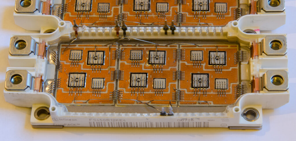
High voltage alone does not automatically require a ceramic package. Many high-voltage gate drivers, isolators, amplifiers, sensors, and power-control ICs ship successfully in molded plastic packages when voltage rating, creepage, clearance, moisture sensitivity, and thermal load are inside the package’s design window.
The packaging decision changes when high voltage is joined by high current, meaningful power dissipation, long hold-off voltage, harsh environment exposure, or a customer qualification requirement that treats moisture, leakage, thermal cycling, and insulation lifetime as system risks. At that point the package is not just a protective shell. It becomes part of the electrical insulation system and part of the heat-removal path.
This is why ceramic packages remain relevant even as plastic packaging has improved. The right question is not “does a high-voltage IC need ceramic?” The better question is: when does the customer need voltage isolation, heat spreading, low leakage, dimensional stability, and hermetic reliability enough to pay for ceramic?
The Short Answer
Ceramic packaging is compelling when the device has to manage several stresses at once:
- High voltage: the package must support creepage, clearance, dielectric withstand, and insulation stability.
- High current: conductors, bond wires, leadframes, clips, or metallized ceramic traces must carry current without excess temperature rise.
- Power dissipation: package thermal resistance becomes a design limiter, not a footnote.
- Hermeticity: moisture ingress can shift leakage, corrode metallization, or degrade sensors, MEMS, RF cavities, and high-impedance nodes.
- Thermal cycling: CTE mismatch among die, attach material, substrate, metal lid, and board can drive fatigue.
- Reliability qualification: automotive, aerospace, medical, industrial, and energy customers often require long-life evidence, not only a datasheet voltage rating.
Plastic packages win when cost, volume, and assembly simplicity dominate. Ceramic wins when the customer is buying reliability margin under combined electrical and thermal stress.
What Ceramic Adds
Ceramic packages give designers a material platform that can combine electrical insulation and heat conduction. That combination is the key. Metals conduct heat but also conduct electricity. Polymers insulate, but thermal conductivity is usually limited. Ceramics such as alumina, aluminum nitride, and silicon nitride sit in the middle: electrically insulating, mechanically stable, and able to move heat better than typical organic package materials.
Aluminum nitride is especially important in high-power packaging because it offers high thermal conductivity while remaining electrically insulating. Public AlN thermal-conductivity work reports room-temperature values around 237 W/m-K for crystalline AlN in research samples, while common power-electronics summaries place polycrystalline AlN ceramic substrates well above alumina. The exact value depends heavily on defects, oxygen, vacancies, grain structure, and processing quality, so package designers should use supplier-specific data rather than a generic headline number.
In power substrates, the distinction is practical. Alumina is lower cost and mature. AlN gives better heat spreading. Silicon nitride is often chosen where mechanical toughness and thermal cycling reliability matter. Direct-bonded copper and active-metal-brazed substrates use a ceramic tile with copper metallization, giving the power module both current-carrying metal and electrical isolation from the heat sink.
What Real Ceramic Package Product Lines Reveal
A public product catalog from a ceramic packaging supplier is useful because it does not present “ceramic package” as one product. It shows the actual package family that appears when customers need different combinations of cavity, routing, sealing, and power handling: HTCC ceramic substrates/packages, CQFN ceramic packages, CSMD power packages, ceramic-metal-plastic lids, plastic air-cavity packages, and CSOP ceramic packages.
The HTCC page is especially relevant. It describes HTCC ceramic substrates and packages as carriers that provide electrical connection, protection, support, and heat dissipation for semiconductor chips. It highlights thermal-expansion matching to semiconductor chips, high-density routing up to 24 wiring layers, tungsten conductors, multiple cavities for partitioning and isolation, harsh-environment suitability, AuSn eutectic attach, seam welding, and hermetic package capability.
That is the real customer language. The demand is not simply “ceramic.” The demand is a package architecture: cavity, lid, metallization, isolation, die attach, sealing, routing density, and thermal path together.
High Voltage Is Not Enough
A low-current high-voltage IC can often stay in plastic. Examples include signal-level isolation, low-power sensing, high-side measurement, and bias-control functions where dissipation is low and the package can meet creepage and clearance requirements. In those cases, ceramic may add cost without solving the customer’s main problem.
The ceramic argument becomes stronger when the package must hold voltage while also moving current and heat. A high-voltage, low-current node is mainly an insulation problem. A high-voltage, high-current node is an insulation, conductor, heat, and lifetime problem at the same time.
This is why many ceramic opportunities are tied to power conversion rather than to voltage rating alone. EV traction inverters, onboard chargers, DC/DC converters, fast chargers, solar inverters, energy-storage converters, industrial motor drives, laser-diode drivers, radar modules, and medical pulser electronics all turn electrical stress into package-level heat and reliability stress.
Material And Package Choices
| Package or substrate class | Why customers use it | Watch-outs |
|---|---|---|
| Alumina ceramic package/substrate | Mature, lower cost, good insulation, strong high-reliability history | Thermal conductivity is much lower than AlN; may limit power density |
| AlN ceramic package/substrate | High thermal conductivity plus electrical insulation; useful for high-power and RF packages | Higher cost; actual thermal performance depends on material quality and process |
| Silicon nitride power substrate | Good mechanical strength and thermal cycling reliability for demanding power modules | Thermal conductivity can be lower than AlN depending on grade; cost and supply matter |
| HTCC ceramic package | Multilayer routing, hermeticity, high reliability, cavity structures, harsh-environment use | Tungsten or moly-manganese metallization has higher resistance than copper; design rules matter |
| CQFN / CLCC / air-cavity ceramic package | Good for RF, MEMS, sensors, optoelectronics, and high-reliability devices needing cavity protection | Not automatically a high-current solution unless the current path and thermal path are designed for it |
| DBC / AMB ceramic power substrate | Combines copper current paths with ceramic isolation for power modules | Thermal cycling, copper thickness, ceramic thickness, and attach process drive reliability |
The customer rarely buys the material alone. They buy a validated combination of material, metallization, lid, attach method, seal, plating, routing, and test data.
Which Customers Actually Need This
The strongest customers are the ones whose systems fail expensively if thermal or insulation margin is wrong.
EV traction, onboard charging, DC/DC, and fast charging are the largest near-term volume opportunity. EV sales exceeded 17 million globally in 2024, according to the IEA, and are expected to exceed 20 million in 2025. Higher battery voltages, SiC traction inverters, faster charging, and bidirectional power conversion all increase demand for packages and substrates that can survive high voltage, high current, and thermal cycling.
Renewable inverters and energy-storage PCS are the second major growth area. IRENA reported 692 GW of renewable capacity additions in 2025, with solar PV accounting for about 510 GW and wind about 159 GW. Solar, wind, and storage systems all need conversion hardware. Ceramic substrates and packages are relevant where outdoor lifetime, high voltage, high current, and service cost justify better thermal and insulation reliability.
AI data-center power infrastructure is a newer but important demand signal. The IEA estimates data centers consumed about 415 TWh in 2024 and projects that consumption to more than double to around 945 TWh by 2030. Not every data-center power IC needs ceramic, but high-current rack power, UPS, backup power, solid-state transformer work, high-density DC/DC conversion, and future medium-voltage distribution can increase demand for better isolation and thermal packaging.
Industrial drives, welding, induction heating, robotics, and factory power supplies are less fashionable than AI or EVs, but they are steady ceramic-package customers. They care about downtime, thermal cycling, surge events, field repair cost, and component availability.
RF, microwave, radar, satellite, aerospace, and defense value ceramic for another reason: cavity structures, RF stability, hermeticity, low moisture sensitivity, and harsh-environment operation. Current may be modest, but leakage, moisture, and dimensional stability matter.
Medical ultrasound, X-ray, piezo drivers, MEMS drivers, and precision high-voltage analog form smaller but higher-value niches. These customers care about high voltage, low leakage, signal integrity, reliability, and regulatory qualification more than lowest package cost.
Where The Growth Is Most Real
The best growth area is not generic “ceramic packages for all high-voltage ICs.” That is too broad. The stronger thesis is ceramic packages for high-voltage, high-current, high-thermal-reliability systems.
EV and renewable power conversion are the cleanest demand drivers because they connect directly to unit growth and power-module content. AI data centers are the most interesting upside driver because power density and grid constraints are forcing a new round of power-architecture decisions. Industrial, aerospace, RF, and medical are steadier, often higher-margin, but less explosive in volume.
For ChinaSemiOps, the practical opportunity is supplier and customer mapping. The valuable work is to identify which customers only need a plastic high-voltage package, which customers need a ceramic cavity package, and which customers need a true power substrate or power module architecture.
What Engineers Should Ask
- Is the problem voltage, current, heat, moisture, or lifetime? If it is only voltage, plastic may be enough. If it is several of these together, ceramic becomes more credible.
- What is the real power dissipation at worst case? Average current can hide thermal stress. Switching loss, conduction loss, surge current, and hot-spot temperature matter.
- Where does the heat actually go? A ceramic material datasheet is not a thermal design. Die attach, substrate thickness, metallization, lid, solder joint, TIM, and heat sink all matter.
- What insulation lifetime is required? With high voltage, the design needs creepage, clearance, dielectric withstand, partial-discharge thinking, and contamination control.
- Does the package need hermeticity? Sensors, MEMS, RF cavities, optoelectronics, and high-impedance analog can fail from moisture or contamination even when the voltage rating looks acceptable.
- What qualification does the customer require? Automotive, aerospace, medical, and energy customers may require thermal cycling, HAST/uHAST, power cycling, isolation testing, and long-duration operating life data.
Caveats
- Ceramic is not automatically better. It can be more expensive, more brittle, and more process-sensitive than plastic.
- AlN has strong thermal potential, but package-level performance depends on the actual ceramic grade, metallization, thickness, attach material, and assembly process.
- HTCC supports high-reliability multilayer packages, but tungsten conductors do not behave like copper. Current path design still matters.
- A ceramic cavity package is not the same as a power module substrate. Do not confuse CQFN/CLCC cavity packaging with DBC/AMB power substrates.
- Growth in EVs, renewables, and AI data centers supports demand for high-reliability power packaging, but it does not automatically translate into demand for every ceramic package supplier.
Closing
High-voltage IC packaging is moving in two directions at once. Plastic packages will keep improving and will continue to win cost-sensitive high-volume sockets. Ceramic packages will keep winning where customers need insulation, heat flow, hermeticity, and lifetime margin together.
The commercial opportunity is therefore not “ceramic replaces plastic.” It is more precise: ceramic packages and ceramic power substrates become valuable in the parts of the semiconductor market where voltage, current, thermal density, and reliability qualification meet.
That is where the customer is willing to pay.
Sources
- Shanghai Xintao Micro New Materials / AlN China, product overview and HTCC ceramic substrate/package page. Used for public supplier examples of HTCC, CQFN, CSMD, air-cavity package, lids, multi-cavity isolation, AuSn, seam welding, and hermetic packaging claims: https://www.alnchina.com.cn/ and https://www.alnchina.com.cn/product/showproduct.php?id=46
- Runjie Lily Xu et al., “Thermal conductivity of crystalline AlN and the influence of atomic-scale defects,” arXiv:1904.00345. Used for AlN thermal-conductivity context and defect sensitivity: https://arxiv.org/abs/1904.00345
- J. Hu, L. Yang, M.-W. Shin, “Thermal And Mechanical Analysis of High-power Light-emitting Diodes with Ceramic Packages,” arXiv:0801.1058. Used for public evidence that ceramic packaging can improve package thermal resistance while creating mounting/process stress tradeoffs: https://arxiv.org/abs/0801.1058
- Andras Vass-Varnai and M. Rencz, “Package Hermeticity Testing with Thermal Transient Measurements,” arXiv:0805.0941. Used for hermeticity and moisture-related reliability context: https://arxiv.org/abs/0805.0941
- IEA, “Global EV Outlook 2025.” Used for EV sales and charging-infrastructure growth context: https://www.iea.org/reports/global-ev-outlook-2025
- IEA, “Energy and AI.” Used for data-center electricity-demand context and AI/data-center power-infrastructure growth: https://www.iea.org/reports/energy-and-ai
- IRENA, “Near-700 GW Surge in 2025 Proves Renewable Energy Resilience,” April 1, 2026. Used for renewable-capacity addition context: https://www.irena.org/News/pressreleases/2026/Apr/Near-700-GW-Surge-in-2025-Proves-Renewable-Energy-Resilience