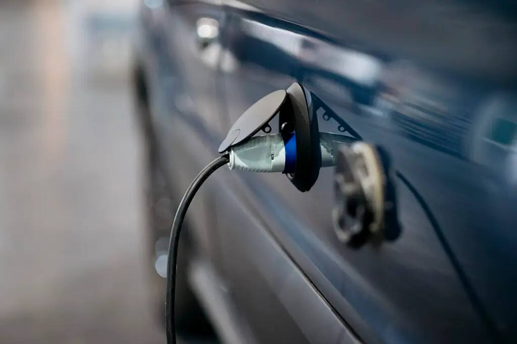
An EV onboard charger makes the isolation problem tangible. AC mains, the traction battery and the controller occupy different electrical domains, so the grid-to-battery boundary must be protected. That safety boundary still does not tell us how every power switch should be driven.
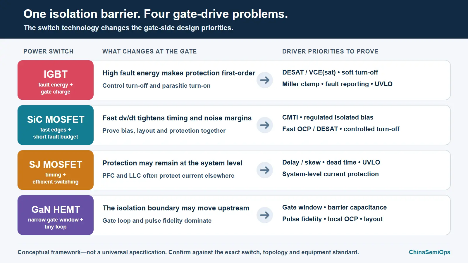
“Galvanically isolated gate driver” is therefore a category label, not a design recipe. An IGBT stage puts fault energy and controlled turn-off near the top of the list. SiC compresses timing and noise margins. A superjunction PFC or LLC stage may place protection elsewhere, while GaN can move the isolation boundary itself.
Three takeaways
- Start with the switch, topology and safety boundary—not a driver catalog.
- Peak source/sink current and headline kVrms are screening numbers, not a complete selection method.
- The useful opportunity is not another generic isolated driver. It is better protection, bias, telemetry and measured proof for demanding power stages.
One label, four selection problems
| Switch technology | Gate-drive problem | Protection and bias emphasis | Isolation/driver architecture to evaluate |
|---|---|---|---|
| IGBT | Larger gate charge, high fault energy, mature industrial and automotive practice | +15 V class turn-on is common; 0 V or negative turn-off may be used; desaturation detection (DESAT/VCEsat), Miller clamp, soft or two-level turn-off, fault reporting and undervoltage lockout (UVLO) are central | Protection-rich isolated smart driver is often a natural fit, subject to working-voltage, surge, creepage and system certification checks |
| SiC MOSFET | Faster edges, tighter short-circuit budget, stronger layout and common-mode sensitivity | Bipolar bias or strong clamp decisions matter; fast overcurrent protection (OCP) or DESAT, controlled turn-off, high common-mode transient immunity (CMTI) and isolated-bias regulation move forward in the checklist | Smart isolated driver plus carefully designed isolated bias is common, but the module, Kelvin source, dv/dt and fault tests decide adequacy |
| Superjunction MOSFET | Efficient high-frequency silicon bridge, often in PFC, LLC or industrial power | UVLO, dead time, propagation delay/skew and external current protection can matter more than IGBT-style integrated DESAT | A dual isolated driver may be enough; protection may live in the controller, current transformer, shunt, comparator or power-stage design |
| GaN HEMT | Narrow gate window, very small gate loop, tight dead time and pulse fidelity | Negative bias is device-specific; local OCP/short-circuit behavior, CMTI, barrier capacitance and layout parasitics dominate | The barrier may be inside an isolated driver, upstream in a digital isolator, or outside an integrated GaN power-stage interface |
Peak current and kVrms do not settle the choice
A 10 A headline does not settle whether a driver fits the stage. Its UVLO rail may not match the switch. Delay and skew may consume the dead-time budget. A DESAT path may react too slowly—or trip on switching noise. Package and pinout may prevent the driver from sitting close enough to the Kelvin source. A lower-current driver can be the better choice when gate charge is modest and clean timing or narrow-pulse fidelity is the harder problem.
Isolation ratings answer different questions. VIOWM is the maximum RMS or equivalent DC voltage the barrier is designed to withstand continuously over its specified life. VIORM is the maximum peak voltage that may appear repeatedly across the barrier during normal operation. By contrast, VISO is usually a short withstand test—often one minute—not a continuous operating-voltage rating. Surge withstand, creepage and clearance are separate checks. These terms follow the definitions summarized in the TI Isolation Glossary.
CMTI answers another question: whether the signal path keeps working through a common-mode dv/dt event. With fast SiC and GaN, isolation capacitance also matters because i = C × dv/dt turns barrier and bias-transformer capacitance into displacement current.
Where each switch changes the design
IGBT usually puts protection first. Analog Devices’ ADuM4135 and TI’s UCC21750-Q1 illustrate why DESAT, Miller clamp, isolated fault signaling, controlled turn-off, UVLO and package spacing remain central. They are not universal answers, but they show the functions an IGBT design must evaluate.
SiC carries much of that protection work into a faster, less forgiving switching environment. Higher dv/dt, negative source transients, short-circuit limits and EMI/loss tradeoffs tie the driver, isolated bias, module layout and fault test plan together. Comparing only amp rating and headline isolation leaves out most of the engineering.
Superjunction MOSFET stages often divide the work differently. A dual isolated driver such as TI’s UCC21520 class can fit a PFC or LLC stage without integrated DESAT, Miller clamp or soft turn-off because current protection may live elsewhere. Fewer integrated protection features do not automatically make that architecture less capable.
GaN can move the isolation boundary
With GaN, the position of the isolation barrier becomes an architecture decision. Three patterns are common:
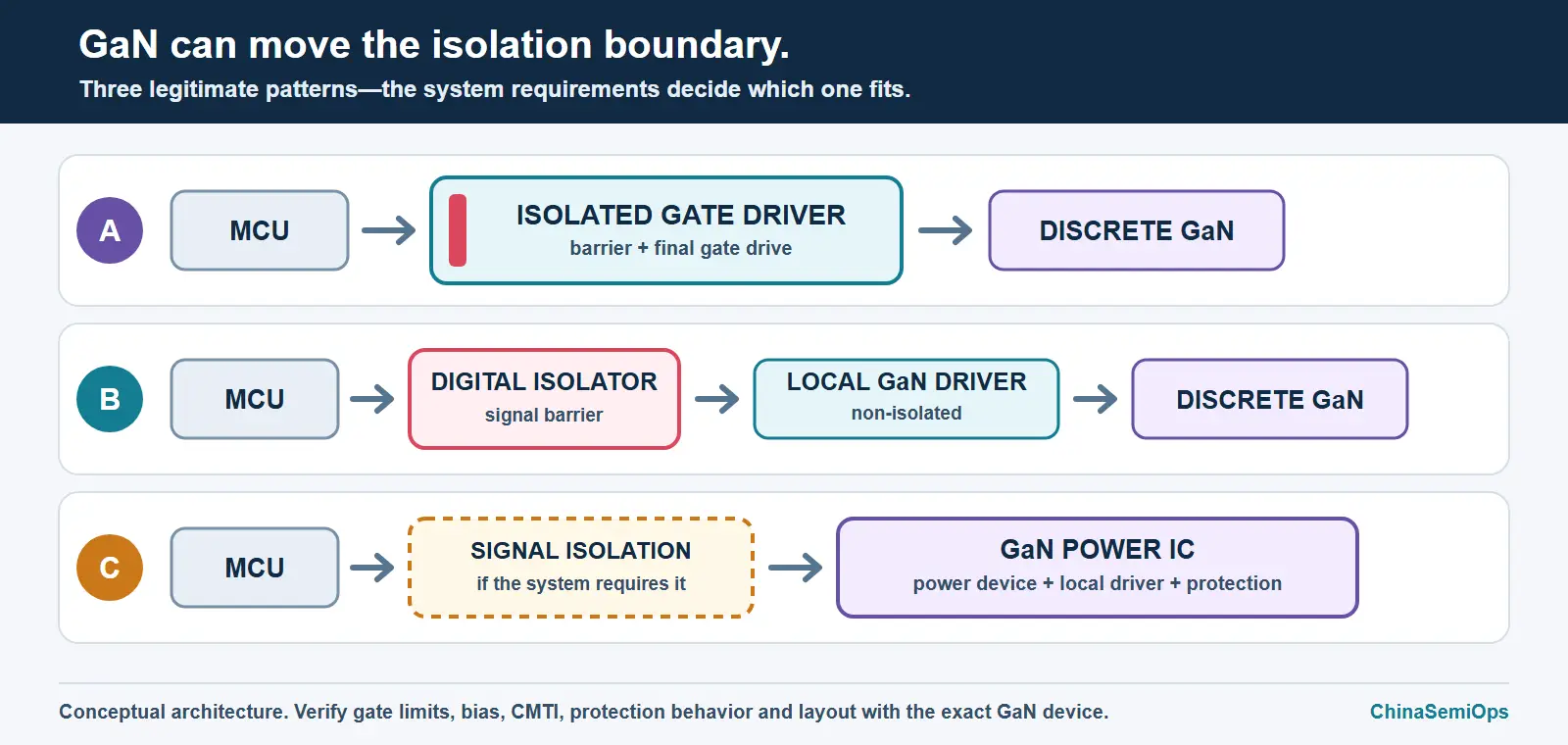
Pattern A uses an isolated driver that matches the GaN device’s gate structure, UVLO, CMTI, isolation class and layout limits. Pattern B moves the final driver close to the gate while a digital isolator and isolated bias provide the barrier. Pattern C keeps the gate loop and some protection inside the power device, leaving controller-interface isolation to the system design. TI’s LMG1210 is a useful non-isolated local-driver contrast, not an isolated-driver recommendation.
China already has drivers; the harder gaps matter more
China does not start from zero. Global suppliers cover smart IGBT/SiC drivers, dual isolated drivers, fast wide-bandgap drivers and isolated bias. Local suppliers also have credible offerings: Chipanalog documents an automotive smart isolated driver, while 3PEAK documents a production reinforced isolated-driver family. “China lacks isolated gate drivers” is not a useful market thesis.
The more interesting work sits in the difficult combinations: fast SiC protection with fewer false trips and controlled turn-off on real modules; regulated isolated bias with monitoring; useful telemetry without unacceptable latency or software burden; and coordination across many floating domains in multilevel or medium-voltage systems. Adaptive drive and programmable slew also need measured EMI, loss, overshoot and fail-safe results—not feature-list enthusiasm.
A practical selection sequence
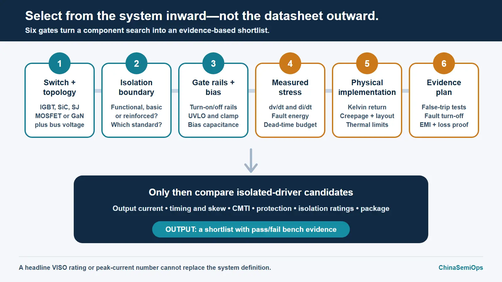
Before opening a driver shortlist, write down six things:
- The exact switch, topology and bus voltage.
- The safety boundary, working voltage and end-equipment standard.
- The gate rails, isolated-bias architecture and acceptable power-up behavior.
- Measured
dv/dt, overshoot, fault energy and protection timing. - The package, creepage, clearance and gate-loop layout constraints.
- The bench evidence, qualification plan and owner for each remaining risk.
Only then compare driver candidates using the same isolation terms and the same pass/fail tests. If your team is defining an OBC, inverter or fast-switching power stage, ChinaSemiOps can help turn a non-confidential operating envelope into a requirements and evidence plan before anyone promises custom silicon or qualification readiness.
Selected primary sources
- TI UCC21750-Q1 — protected isolated gate-driver functions and explicit isolation terms.
- Analog Devices ADuM4135 — an IGBT-oriented smart isolated-driver baseline.
- TI Isolation Glossary — definitions of working, repetitive-peak, transient, withstand and surge isolation ratings.
- TI UCC21520 — dual-channel isolated-driver architecture.
- Analog Devices MAX22701D — fast isolated wide-bandgap driver-family evidence.
- Chipanalog CA-IS3215ENW-Q1 — China smart isolated-driver evidence.
- 3PEAK TPM23513B — China reinforced isolated-driver evidence.
- TI LMG1210 — non-isolated GaN/MOSFET local-driver contrast.
Related ChinaSemiOps insights
- GaN Gate-Driver IC Opportunities in Robot Joints
- Where Solid-State Transformers Create Real Power-IC Opportunities
- Where HVAC Growth Creates Semiconductor Opportunities
Disclosure: This is a public-source engineering analysis and selection framework, not a product qualification or component recommendation. Verify ratings and protection behavior against the current datasheet, exact switch, layout and end-equipment standard.