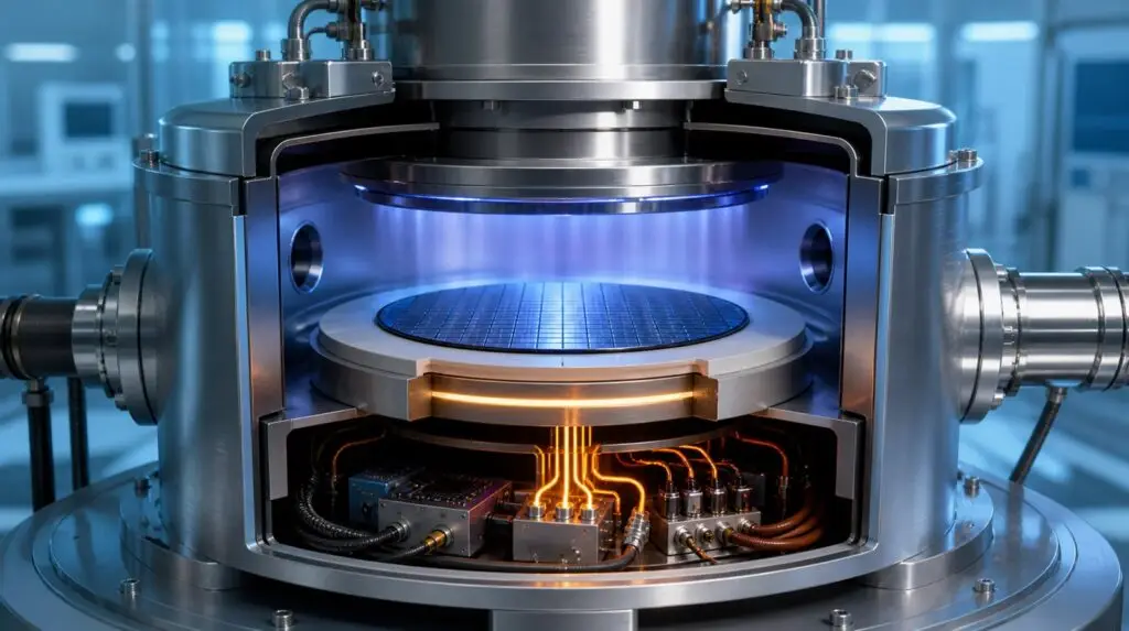
An electrostatic chuck (ESC) is the electrically biased platform beneath a wafer in many semiconductor process chambers. It holds the wafer without a mechanical clamp and helps maintain the controlled thermal interface needed during processing. Engineers who work mainly on IC products may rarely encounter the term because the chuck, high-voltage supply and control loop are buried inside the tool.
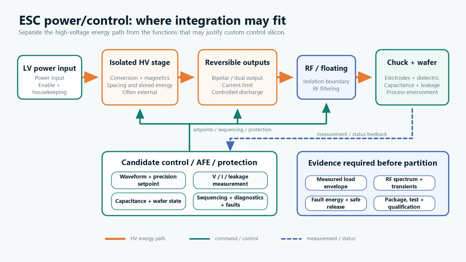
The design problem is not simply generating a few kilovolts at low current. The system must clamp the wafer predictably, detect its state, tolerate radio-frequency (RF) energy and plasma bias, limit fault energy, and remove residual charge before release. That makes the ESC a useful example of where high-voltage analog control may matter even when the final multi-kilovolt stage remains external.
Three takeaways
- Start from the load: electrode topology, chuck dielectric, wafer, leakage and capacitance define the job; voltage alone does not.
- Control creates much of the differentiation: clamp/de-chuck sequencing, sensing, current limiting, interlocks and diagnostics can matter as much as conversion.
- Prove the silicon boundary: controller, analog front end (AFE), isolation and protection functions may integrate, while the multi-kilovolt stage, magnetics, spacing and qualification may remain external.
What the ESC drives electrically
An ESC embeds one or more electrodes in a dielectric chuck beneath the wafer. The resulting capacitive and leakage path changes with chuck construction, wafer condition, temperature and process environment. The supply must charge it, hold a controlled state and later remove or reverse charge.
Public patent evidence: an Applied Materials patent discloses source/sink operation and voltage adjustment using leakage-current or wafer-potential feedback. It is an implementation example, not proof of current commercial topology.
Maximum voltage is therefore not enough. Capacitance sets charging current and settling; leakage affects measurement and fault thresholds; residual charge makes de-chucking a controlled operation rather than a simple output-off command.
Follow the wafer through one electrical cycle
1. Detect and prepare. Check interlocks and a wafer-state indicator before applying full clamp voltage.
2. Clamp with a defined profile. Ramp, offset or shape the voltage while controlling current and stored energy.
3. Monitor during process. Define filtering, isolation, measurement bandwidth and fault thresholds in the presence of RF, plasma bias and fast transients.
4. De-chuck and verify release. Reversal, ramp-down, grounding or active discharge may be needed; “zero volts commanded” does not prove safe release.
What public supplies reveal
The following specifications are manufacturer-stated and should be checked against the current datasheet before design use. They establish a public operating envelope; they do not reveal shipment volumes, internal BOMs or buyer preferences.
| Public product example | Vendor-stated envelope | Control clue |
|---|---|---|
| Advanced Energy Trek 646 | 0 to ±3 kV, ±6.5 mA | Stored profiles, wafer-state thresholds and custom clamp/de-clamp waveforms |
| Advanced Energy Trek 645 | Two equal-and-opposite outputs, 0 to ±2 kV, ±6.5 mA DC | Leakage and capacitance monitoring, programmable waveforms and HV interlock |
| Matsusada EJC | Models from ±1 to ±5 kV | Reversible polarity, 100 ms response and optional RF filters |
| Spellman ESC Series | Ground-referenced reversible and floating bipolar configurations | Current limiting, fault diagnostics and HV safety interlock |
The recurring pattern is reversible high voltage at modest current, combined with measurement and state control. The exact voltage, channel count, floating requirement and RF environment remain application-specific.
Use an operating-envelope worksheet before choosing the architecture
| Input to obtain | Architecture consequence | Evidence to request |
|---|---|---|
| Chuck and electrode topology | Monopolar, bipolar, floating and channel-count choice | Chuck construction and chamber interface |
| Clamp voltage and polarity | Output range, isolation and level shifting | Minimum, nominal and maximum over temperature |
| Capacitance and leakage | Charging current, settling, measurement floor and stored energy | Measured range across wafer and chuck life |
| Clamp/de-chuck waveform | Reversal, arbitrary waveform, grounding and timing | Waveform plus pass/fail release criteria |
| RF and plasma-bias environment | Filtering, common-mode range and transient immunity | Spectrum, bias and maximum transients |
| Wafer-state detection | Current/capacitance AFE and calibration | Thresholds and false-positive limits |
| Arc, short and open response | Limiting, shutdown, discharge and event logging | Fault energy and safe-restart sequence |
Where custom high-voltage analog may—and may not—fit
ChinaSemiOps inference: credible integration candidates include waveform and setpoint generation, voltage/current sensing, wafer-state measurement, isolated communication, sequencing, diagnostics and fault protection. The complete supply is a different claim: multi-kilovolt output devices, magnetics or multipliers, RF filters, discharge paths, spacing, connectors and tool qualification may remain discrete, hybrid or modular.
What public part numbers do—and do not—prove
In this bounded public-source review, no current catalog IC explicitly marketed for ESC was located. These examples show real circuit functions—not production BOMs or recommended parts.
- Transformer-primary drive: a TEL patent gives an exemplary channel using an XR-2207 and a counter-phase pair of OPA541AP amplifiers to drive a step-up transformer. This is a historical example, not a shipped BOM.
- Isolated current feedback: a Lam Research patent names AD202KY and OP490GP. The AD202 is obsolete; OP490 is not recommended for new designs.
- Multi-kilovolt module: the Applied Materials patent names an EMCO F30. Separately, XP Power currently lists an F30 rated 10 W, 0–3 kV and 3.3 mA. The current listing is a module—not an IC—and does not prove continuity with the patent-era unit or current ESC use.
- Modern adjacent signal chain: Analog Devices’ CN0586 combines AD5754R, ADHV4702-1, LT8365 and ADuM4151. It supports ranges including ±100 V and states drive capability up to 20 mA; actual current depends on voltage, thermal conditions and the ADHV4702-1 safe operating area. It illustrates upstream control, not a kilovolt ESC stage.
Voltage and isolation labels still need care: continuous working voltage is not the same as one-minute withstand or surge voltage. Our guide to SOI versus BCD for high-voltage analog explains why the real voltage class and isolation strategy come before process selection; voltage alone does not automatically require ceramic packaging.
Open questions: commercial ESC-box converter topologies and BOMs are generally not public. Neither are the volumes, NRE economics, qualification ownership or willingness of a subsystem maker to replace catalog or FPGA/MCU control with custom silicon. Those must be established with a specific non-confidential operating envelope.
Selected primary sources
These public sources support the application and product examples used above. They establish disclosed functions and operating envelopes—not market size, shipment volume or a universal ESC architecture.
- TEL, US20100061033A1 — historical transformer-primary waveform and amplifier example.
- Lam Research, US5933314A — historical isolated current-sense and feedback example.
- Applied Materials, US6198616B1 — disclosed source/sink operation and leakage-current or wafer-potential feedback.
- Analog Devices, CN0586 — modern adjacent 200 V-span bipolar signal-chain reference.
- Advanced Energy, Trek 646 — bipolar output envelope, stored profiles and wafer-state control functions.
- Matsusada Precision, EJC Series — reversible polarity, model voltage ranges and optional RF filtering.
- Spellman, ECHUCK Series — ground-referenced and floating bipolar configurations, current limiting and fault controls.
Questions that determine the architecture
An ESC power architecture depends on electrode topology, voltage, capacitance, leakage, clamp and release waveforms, RF/DC-bias conditions, state detection, fault cases and qualification ownership. Several of these values are normally proprietary and could not be established through public-source research alone.
Working on ESC power or control? ChinaSemiOps welcomes non-confidential technical feedback and application requirements from equipment, subsystem and IC teams. We are evaluating where high-voltage analog IC design services could be relevant; this article does not claim prior ESC deployment or tool qualification.
Disclosure: This article is a public-source engineering analysis. Product figures are manufacturer-stated and subject to current datasheets and operating conditions. The functional partition is a ChinaSemiOps inference, not a teardown or proof of a commercial IC socket. The featured image is an AI-generated, vendor-neutral editorial illustration created for ChinaSemiOps; it is not a photograph, product teardown or depiction of a specific commercial tool.