BMW sixth-generation electric-drive units on display in Munich, September 2025. This is a generic illustration of an electric-vehicle drivetrain. The photograph does not show which power semiconductors, voltage class or suppliers are used inside, and it implies no connection to the Wolfspeed–BorgWarner announcement discussed below or endorsement by BMW. Photo: Alexander Migl / Wikimedia Commons, taken September 7, 2025, CC BY-SA 4.0 (Creative Commons Attribution-ShareAlike 4.0 International). That license applies to the photograph itself and is not limited by the republication notice at the end of this article.
Suppose a supplier tells you that the transistors in your electric-vehicle (EV) traction inverter are 1200-volt (1200 V) silicon carbide (SiC) parts, and that the platform is called 800 V. Does that leave 400 V for switching spikes? That is a voltage budget question, and the two labels alone cannot answer it. A traction inverter is the power converter that turns the battery's direct current (DC) into the alternating current that drives the motor. SiC is a compound semiconductor used to build fast, efficient power switches.
No. The subtraction 1200 − 800 = 400 is arithmetic, not margin. A voltage budget starts with the highest voltage the inverter's local DC link (the supply connection to its switches, with a capacitor close by) can reach, adds what happens at the transistor's own terminals while it switches, and compares that peak with the limits of the exact part under its stated conditions. The design owner's written headroom policy then decides whether the result is acceptable. In this article a voltage budget means that evidence record, not a single number.
Three takeaways
- An 800 V platform label and a 1200 V blocking rating are two labels, not a measured margin. Neither tells you the highest voltage a transistor actually sees.
- Keep three records apart: the maximum voltage at the local DC link, the measured peak across the transistor's own terminals during switching, and the exact part's limits with their conditions.
- Only the responsible design owner's written headroom policy turns that comparison into an acceptance decision. None of the sources used here supplies a universal percentage.
What the 800 V/1200 V pairing establishes
Vendor statement: On October 28, 2026, Wolfspeed announced a multiyear supply agreement for its SiC devices to support BorgWarner's next-generation 800 V SiC-based inverter platform, and said that BorgWarner is leveraging Wolfspeed's 1200 V SiC technology for that platform (Wolfspeed announcement).
That is a company statement about a commercial pairing. It names no part number, maximum DC-link voltage, switching measurement, internal circuit topology or qualification result, so it is not evidence of an independently tested design. BorgWarner's own power-electronics page, which is undated, lists an 800-volt SiC inverter and, separately, other platforms. It does not connect its product images to the agreement or to a 1200 V part.
What the pairing does show is how the labels are used. "800 V" names the platform. "1200 V" is a blocking rating: the off-state voltage a part is specified to withstand under stated conditions. For a MOSFET (metal-oxide-semiconductor field-effect transistor), the gate-to-source voltage controls current between the drain and source, the main-current terminals. The blocking rating refers to the drain-to-source voltage in the off state. A blocking rating is a limit under defined conditions, not an operating setpoint.
Open question: whether "800 V" is a nominal reference or a limit for this platform is for the platform's owner to say. Ask for the definition before using the number.
Find the maximum voltage at the local DC link
The DC link, also called the DC bus, is the connection that carries the battery's direct current to the inverter's switches. A local capacitor sits close to those switches, and its voltage is what the transistors see before any switching event adds to it. A nominal voltage is a reference or class value. A maximum voltage is the highest value specified for a defined scenario and duration. The two are not interchangeable.
Mitsubishi Electric's industrial application note works in the same order: it determines a module's voltage rating from the input supply voltage or the bus voltage applied across the module (section 8.1.1 of the February 2024 edition). That note is industrial guidance, so its worked examples are not automotive limits.
Ask the vehicle manufacturer or inverter integrator for the maximum local DC-link voltage in each case below, with its duration and where it was measured or specified:
- the battery at full charge across its temperature range, including production tolerance;
- regenerative braking, when the motor returns energy to the DC link;
- start-up, shutdown, pre-charge (charging the DC-link capacitor gradually) and disconnect;
- protection thresholds and how long protection takes to act;
- specified fault cases, kept apart from normal operation.
A battery-terminal figure is not automatically the capacitor voltage at the instant of switching. If a stated maximum already includes ripple (the small repetitive voltage variation on the link), do not add ripple again. Our article on EV traction-battery protection covers pre-charge, high-current contactor switches and fault disconnect, which feed several of these cases. Wolfspeed's announcement discloses none of these values.
Measure device-terminal stress in the commutation loop
In a common arrangement, an inverter switches current between two transistors stacked across the DC link. That arrangement is a half-bridge: the high-side transistor (QH) connects to DC+, the low-side transistor (QL) connects to DC−, and the load, such as a motor winding, connects at the midpoint, called the switch node (SW). When one transistor turns off, the current has to move to another path very quickly. That handover is commutation.
The commutation power loop is the path the fast-changing current takes: from the local capacitor, through QH, the switch node and QL, and back to the capacitor. It is a different path from the gate loop, which carries the small control current from the gate driver to a transistor's gate terminal and back through that transistor's source connection. A separate source connection for the gate driver, called a Kelvin-source return, keeps the large power current out of the gate path. It reduces coupling between the two loops but does not remove it. Isolation, an insulation barrier between voltage domains such as a driver's control side and the power side, is a third matter with its own rating, separate from the transistor's drain-source blocking rating.
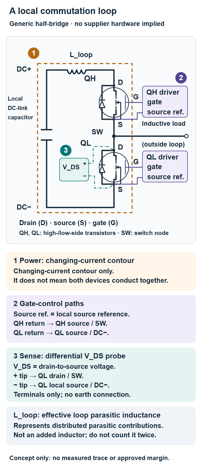
Every conductor in the loop has stray inductance, an unintended property that resists fast current changes. Where current changes quickly, that inductance produces a voltage. Inference: as a first-order screening estimate, the size of that inductive voltage contribution, written ΔV_ind, is ΔV_ind ≈ L_loop × |di/dt|. Here L_loop is the effective stray inductance of the whole loop, di/dt is how fast the current changes with time, and the vertical bars take its magnitude. Inductance in henries (H) times current change in amperes per second (A/s) gives volts (V). In more convenient units, nanohenries (nH) times amperes per nanosecond (A/ns) also gives volts: 1 nH × 1 A/ns = 1 V. Mitsubishi writes the relation as ΔV = di/dt × L; the approximation and magnitude notation are ours.
This is one contribution, not the terminal peak. Circuit polarity and the switching state decide whether it raises or lowers a particular terminal's voltage. The real peak also depends on the transistors' own capacitances, coupled inductances, any snubber or clamp (circuits added to limit voltage spikes), and how the measurement is made. Vendor statement: Semikron Danfoss International writes that when stray inductance is too high, high voltage overshoots (peaks above the intended level) may occur as the device switches off, potentially causing damage (Application Note AN 26-002, Revision 01, April 14, 2026). Mitsubishi names wiring inductance and switching speed as the causes of surge voltage, a brief spike above the normal level. Both notes describe their own industrial modules, and none of their numbers transfers to an 800 V vehicle inverter.
Be careful about where the loop ends. In Mitsubishi's circuit figure, L1 is only the wiring between the smoothing capacitor and the module. The loop that matters also includes the module's internal paths and the capacitor itself, so count each contribution once.
There are two ways to build the evidence, and they are alternatives, not additions. Prediction estimates a specified switching edge from a model and then validates it by measurement. Measurement records the peak with a differential probe (one that measures the voltage between two points rather than from ground) attached directly across the low-side transistor's drain and source, as in the figure, for a stated event. Check the probe's differential-voltage limit (between its two tips) and common-mode limit (the voltage shared by both inputs relative to the probe's specified reference), including any applicable transient limits, against the stated measurement conditions. Also check any separately specified limit from each input to the probe's reference, any frequency dependence of the common-mode rating, and the ratings of the actual leads and tips. Record its bandwidth and loading. If that trace already contains the overshoot and ringing (the oscillation after the edge), do not add ΔV_ind or a ringing allowance for the same event.
State what limits the measurement itself. The probe and oscilloscope have finite gain and offset accuracy, bandwidth (the range of frequencies they follow), loading (the probe changes the circuit it measures), and reference and setup effects such as lead length. Show that the ringing is real and not pickup (noise coupled into the probe or its leads). That is measurement uncertainty. It is a different thing from coverage: how many parts, temperatures, aging states and operating points the tests included. Record how you combine the two, and do not assume they are statistically independent. Also record where you measured. The terminals you can reach are not the semiconductor chip (die) inside the module, and the two references are not interchangeable.
Compare the peak with exact part limits and conditions
Take the exact device or module, driver variant and current datasheet edition, and write down each limit with the conditions it applies under: temperature, gate bias (the voltage applied to the gate), pulse duration, repetition and polarity. Then compare like with like:
- the off-state drain-source voltage limit, and whether it is an absolute maximum (a value that must not be exceeded under the stated conditions) or a recommended operating value;
- any transient or repetitive allowance the datasheet states explicitly. The absence of a rating is not an allowance;
- gate-source limits, which are a separate check;
- short-circuit and protection turn-off limits, and avalanche capability (the ability to survive being driven into breakdown) only where the part specifies it;
- driver, capacitor, clamp and snubber constraints.
Normal switching and fault events are separate evidence. An ordinary turn-off happens repeatedly inside the operating envelope. A fault such as a short circuit or a disconnect under load has its own current, energy, duration and protection sequence. A single absolute maximum value does not establish reliability at that voltage, and slowing an ordinary edge does not prove safe fault interruption.
If the comparison looks tight, mitigation options exist, but they depend on the hardware. Layout changes reduce L_loop: Semikron Danfoss shows capacitor and busbar (flat power conductor) arrangements that change the loop area in its modules. Slower switching reduces di/dt, but it needs evaluation of loss, ringing and protection, and Semikron Danfoss notes that the gate resistor of its integrated-driver module cannot be adjusted. A snubber is a small circuit that absorbs switching energy to limit voltage spikes. Mitsubishi warns that its simplest capacitor-only type can resonate with the loop inductance, and it says to select a circuit after actual evaluation, with the snubber leads kept short. The improvement figures and examples in those notes belong to their own modules and do not carry over.
Open question: how much headroom is enough? Only the design owner can answer, in writing, including how temperature, aging, part-to-part spread and measurement uncertainty are covered. The sources used here supply no universal percentage, and 400 V is not one. Do not add the same effect twice: if the stated DC-link maximum includes ripple, or the measured peak includes ringing, leave them out of any further allowance.
Build the five-row voltage-budget evidence record
Fill in one record for each device and each switching event, and leave unknowns blank. A blank cell is information.
| Record row | Evidence to attach | Usually supplied by | It does not show |
|---|---|---|---|
| 1. Local DC-link envelope | Maximum DC-link voltage per scenario, with duration, location and tolerances; regenerative, start-up, shutdown and fault cases kept separate | Vehicle manufacturer; inverter integrator | Switching spikes at the transistor |
| 2. Exact part limits | Datasheet edition; drain-source limits with conditions; absolute versus repetitive; fault and protection limits | Device supplier | What your circuit actually reaches |
| 3. Switching and protection measurements | Terminal V_DS peak including ringing at stated DC-link voltage, current, temperature and gate settings; probe point, bandwidth, loading; uncertainty and coverage | Test and release team | Other operating points; fault-energy capability |
| 4. Loop, driver and mitigation constraints | Defined L_loop boundary and how it was extracted; current slew; gate-resistance and snubber options; loss and thermal effects after any change | Module and driver integrator; inverter integrator | A measured peak |
| 5. Accepted policy and disposition | Written headroom policy; treatment of temperature, aging, spread and uncertainty; named decision, owner and date | Responsible design owner | That rows 1 to 4 are correct |
Next action: for one transistor and one switching event, fill in rows 1 to 3 first, then ask the design owner to compare them under the policy in row 5. Rows 1 to 3 are specifications, measurements and datasheet facts; rows 4 and 5 explain and judge them. The record is a way to organize evidence. It grants no design signoff and states no real vehicle's budget. The same requests apply to any supplier, in any country.
This article is educational. It does not recommend a part, state any manufacturer's actual voltage budget, or replace a design review or qualification process.
Selected primary sources (checked November 2, 2026)
- Wolfspeed: Wolfspeed Powers the Future of EVs with Multiyear Silicon Carbide Device Agreement (October 28, 2026) supports the dated vendor statement of the 800 V platform and 1200 V SiC technology pairing.
- Semikron Danfoss International: Application Note AN 26-002, Revision 01, April 14, 2026, Silicon Carbide Specific Considerations for SKiiP, a Semikron Danfoss power-module family supports the stray-inductance, turn-off overshoot and layout discussion for its industrial modules.
- Mitsubishi Electric: Industrial Full SiC Power Module Application Note (February 2024 edition) supports the loop-inductance distinctions, the surge-voltage relation and the snubber guidance.
- BorgWarner: Power Electronics (undated product page) supports only the application context of an 800-volt SiC inverter in its portfolio.
These two dated application notes discuss industrial modules. They do not establish the hardware inside the announced automotive inverter. Confirm the edition you rely on with its publisher.
Please link to this article when sharing. Contact us for permission to republish the full article.