Solid-state transformers create real semiconductor opportunities—but the near-term IC value sits mainly around the main energy path, not inside a single “transformer chip.”
For power-IC engineers and product planners, the useful decision is architectural: power modules and high-frequency magnetics carry the medium-voltage energy, while isolated gate drive, bias power, sensing, protection, supervision and communications create plausible integrated-device sockets. Public 2025–2026 evidence shows serious product development; named commissioned sites with operating histories remain less visible.
Three takeaways
- Confirmed: current public reference designs and supplier portfolios place SiC switches or modules, magnetics, insulation and cooling in the main power path.
- Confirmed: gate-driver, sensing, control, communications and auxiliary-power products are identifiable support-layer semiconductor content.
- Inference: the clearest custom-IC openings are in integrated drive, measurement, protection and distributed control—but only after an OEM architecture defines voltage domains, channel count and qualification requirements.
What an SST changes
A conventional transformer changes voltage magnetically at grid frequency. A solid-state transformer adds high-frequency switching, filtering, one or more DC links, a medium- or high-frequency isolation transformer, and digital control. That enables regulated and potentially bidirectional power flow, multiple ports and faster system control, but it also adds switches, sensing, software, insulation coordination and fault-management complexity.
The exact circuit varies. Public designs use building blocks such as active front ends, cascaded H-bridges, dual-active bridges and multilevel stages. The U.S. Department of Energy’s roadmap frames solid-state power substations as modular power-electronic building blocks, while INL’s February 2026 overview describes SST conversion through high-frequency semiconductor switching, filtering and a smaller transformer. These are architecture references—not proof that one topology has won.
Productization is ahead of deployment evidence
Vendor-stated: Infineon and DG Matrix announced a SiC partnership for SST platforms serving AI data centers and industrial power. Microchip introduced 3.3 kV SiC power modules explicitly positioned for SSTs. Enphase announced development of a 1.25 MW-rack IQ SST architecture for 800 VDC data centers and said demonstrations, pilots and volume shipments were expected in later stages. Those announcements establish investment and productization activity; they do not, by themselves, establish a broad installed base.
For the adjacent data-center path, see where custom analog and power ICs re-enter the 48 V-to-800 V stack.
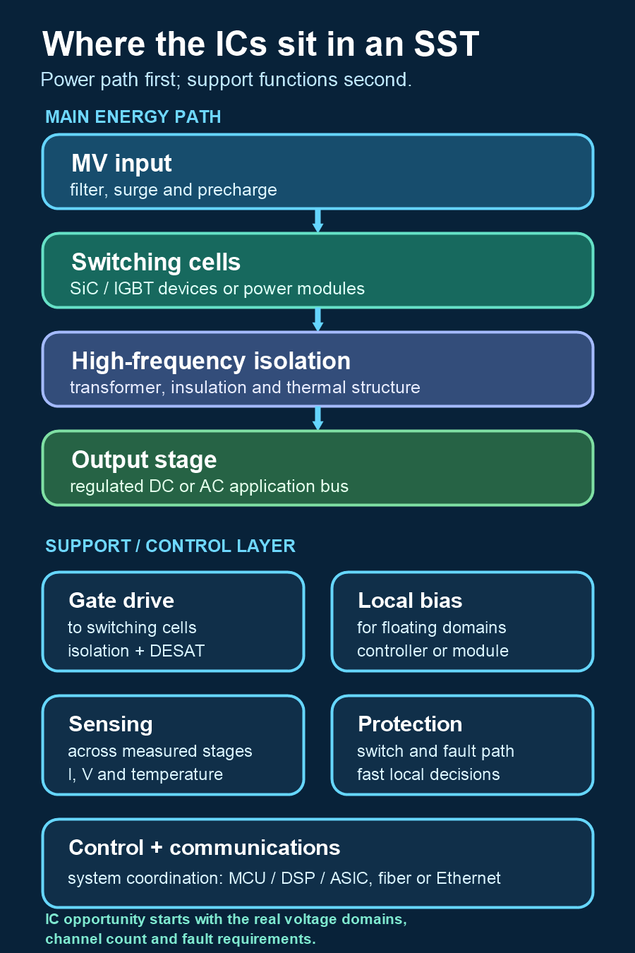
Confirmed engineering evidence: TI’s 50 kW modular SST reference design is especially useful because it exposes the partition rather than only the headline. Its cascaded H-bridge and dual-active-bridge implementation combines 3.3 kV-class SiC power hardware, a high-frequency transformer, isolated gate-drive boards, local bias power, isolated current/voltage/temperature sensing, fast fault comparison, real-time controllers, fiber links and Ethernet communications. It is a laboratory reference design, not a commissioned commercial deployment.
Power modules carry the energy; ICs surround it
Current public medium-voltage SST architectures do not collapse the power path into one monolithic chip. The constraints span switch voltage and current, module thermal paths, magnetic design, bus structures, creepage and clearance, EMI and fault energy. Even a gate-driver isolation rating is not permission to place one driver across an entire 15 kV or 35 kV system boundary; working voltage, surge, altitude and insulation lifetime must be allocated for each cell and barrier.
Supplier product pages show the boundary. An active isolated gate-driver IC such as TI’s UCC21750 drives and protects an external SiC or IGBT switch; TI’s preview UCC218915-Q1 is instead an isolated pre-driver that drives an external NMOS/PMOS buffer. An isolated sensing IC transfers a low-voltage representation across its barrier, while an external divider, shunt or transducer still interfaces to the power node. Auxiliary bias may use a transformer-driver IC plus external magnetics, or an isolated DC/DC module containing an integrated transformer. These are different product types and should not all be called monolithic analog ICs.
Vendor-stated development evidence: Enphase says its developing IQ SST uses a custom 22 nm “Kestrel” control ASIC across hundreds of coordinated power modules. That is direct evidence for SST-specific control silicon—but not for a monolithic chip carrying the medium-voltage power.
Where the support-semiconductor sockets are
| Function | Likely implementation | Evidence state | Next proof |
|---|---|---|---|
| Main MV energy path | SiC/IGBT switches or modules, magnetics, bus and cooling | Direct reference-design evidence | Rated topology and fault envelope |
| Gate drive and bias | Isolated driver/protection IC plus bias controller or isolated-power module | Direct product and reference-design evidence | Working voltage, CMTI, channel count and lifetime |
| Sensing and local protection | Isolated modulator/amplifier, comparator, Hall sensor and temperature monitor | Direct reference-design evidence | Accuracy, latency, divider/shunt and safety allocation |
| Control and communications | Real-time MCU/DSP, fiber/digital isolation, Ethernet; sometimes custom ASIC | Direct design evidence; ASIC is vendor-stated | Partition ownership, redundancy and cybersecurity |
| Per-module supervision | Local measurement, fault logic and isolated communication | Architecture-supported | Exact submodule voltage and OEM partition |
| Partial-discharge or arc AFE | Undetermined | Not established as a standard SST IC socket | Named detection requirement and qualification method |
The battery-monitor shortcut is particularly risky. A battery-monitor IC may fit an SST-plus-storage system, but it does not prove a standard converter-cell monitoring socket. The public design must first show that electrochemical storage and its series cells are actually inside the product boundary.
Use a proof ladder for commercial claims
For market screening, separate five levels: research prototype, working reference design, announced product, customer pilot, and commissioned installation with operating history. Supplier partnerships and product pages are valuable signals, but they should not be reported as deployments. Likewise, a compatible gate driver or sensor is an architectural fit—not a disclosed design win.
This distinction changes the opportunity ranking. Main-path SiC devices and modules are clearly important but require materials, packaging and high-power qualification capabilities. For an analog or mixed-signal IC team, the support layer is a more credible entry point. Differentiation still depends on customer-specific CMTI, protection latency, sensing accuracy, isolation lifetime, channel density, diagnostics and functional partition.
For a related high-voltage comparison, see why protection—not the switch—is becoming the battleground at high voltage and high current.
Start with five buyer-specific questions
- Which architecture and application is real: data-center 800 VDC, charging, grid support, storage or another system?
- What are the cell voltage, switch technology, power level and number of floating domains?
- Which faults must be detected locally, and what shutdown latency and fault energy are allowed?
- Who owns the function—the power-module supplier, converter OEM, controller team or site integrator?
- What insulation, EMC, thermal-cycling, reliability and safety evidence is required before qualification?
The practical next step is to map one named SST architecture by voltage domain, switch count, isolation boundary, sensing channel and fault requirement before discussing a custom IC. That one-page map will show whether the real opportunity is an isolated gate driver, sensing/protection AFE, auxiliary-bias device, controller ASIC—or no custom IC at all.
Primary references
- U.S. Department of Energy — Solid State Power Substation Technology Roadmap
- Idaho National Laboratory — Solid-State Devices and the Power Grid
- Texas Instruments — 50 kW SiC Modular SST Reference Design
- Texas Instruments — TIDA-011012 Design Guide
- Texas Instruments — UCC21750 Isolated Gate Driver
- Texas Instruments — UCC218915-Q1 Isolated Gate Predriver and Protection IC
- Infineon — Solid-State Transformer Application Portfolio
- Infineon — DG Matrix SiC Partnership Announcement
- Microchip — 3.3 kV SiC Modules for SST Applications
- Enphase — IQ SST Development Announcement
- Jeong et al. — 13.2 kV Class Three-Phase SST Prototype and EtherCAT Control
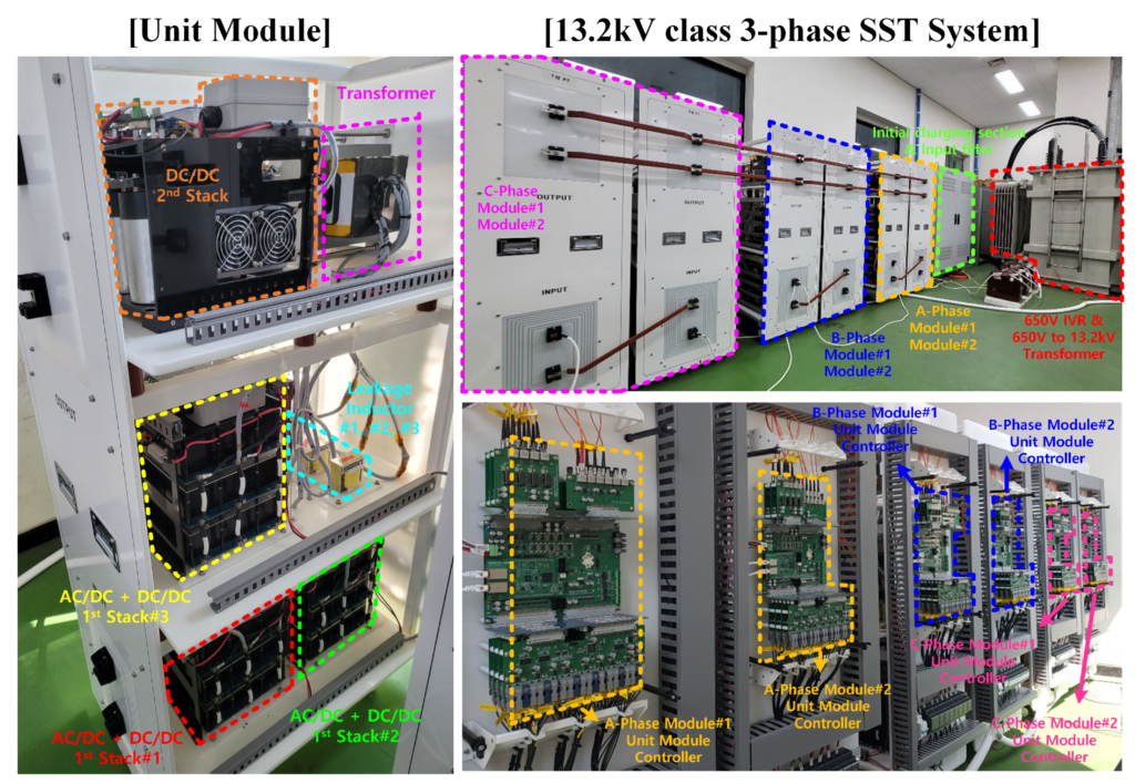
Featured image: Figure 6 from Jeong, Yun, Park, Kim, Ryu, Baek and Kim, Electronics 11(19), 3092 (2022), used under CC BY 4.0. The figure shows a real 13.2 kV-class three-phase SST prototype and its unit modules; it is not a ChinaSemiOps product or customer installation.
Disclosure: This is a public-source architecture and market-screening analysis. Vendor announcements are labeled as vendor-stated, and opportunity rankings are ChinaSemiOps inferences. It does not establish customer programs, design wins, qualification, field deployment or production readiness. Sources were checked through 10 August 2026.