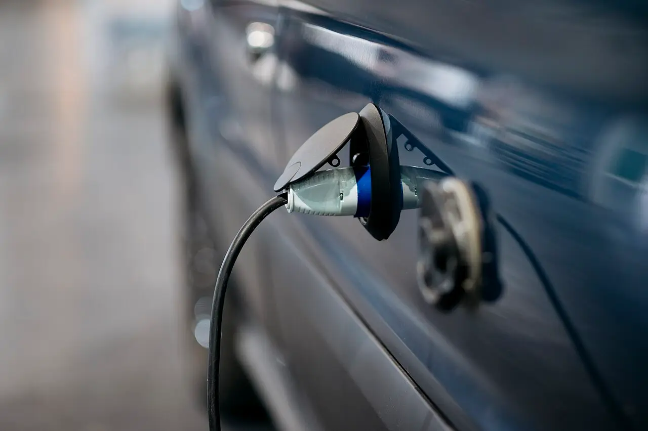
An EV (electric vehicle) onboard charger makes the isolation problem concrete. It converts AC (alternating-current) mains power into DC (direct-current) power for the traction battery, and the DC output is isolated from the grid. An isolation barrier, a gap with no direct conductive path, provides that separation. Where the controller sits, on the high-voltage side or the low-voltage side, decides which gate commands must cross a barrier.
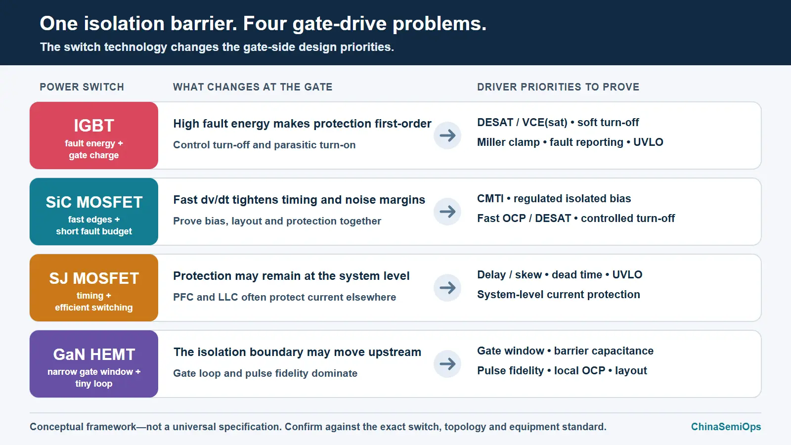
That barrier does not tell you how each power switch should be driven. A galvanically isolated gate driver is a chip that carries the on/off command across a barrier and drives the switch’s gate, its control terminal. When the controller sits on the same side as the switch, a non-isolated driver may be enough. What the driver must do depends on the switch:
- an IGBT (insulated-gate bipolar transistor), a high-current switch where fault energy and controlled turn-off come first;
- a SiC MOSFET (silicon-carbide metal-oxide-semiconductor field-effect transistor), which switches fast and leaves little timing and noise margin;
- a superjunction (SJ) MOSFET, a silicon MOSFET with a charge-balanced structure, with PFC (power factor correction, which makes the current drawn from the mains a sinusoid in phase with the mains voltage) and LLC (inductor–inductor–capacitor resonant converter, a circuit with two inductive elements and one capacitor) stages among its documented application examples, where protection may sit elsewhere;
- a GaN HEMT (gallium-nitride high-electron-mobility transistor), which has a narrow gate-voltage window and can move the isolation boundary itself.
Three takeaways
- Start with the switch, the topology and the safety boundary, not with a driver catalog.
- Peak source/sink current (the largest gate current the driver can push out or pull in) and the headline isolation voltage in kV RMS (kilovolts, root-mean-square, the effective value of an AC voltage) are screening numbers. Each isolation rating answers a different question, so read it with its waveform, duration and test conditions.
- Generic isolated drivers already exist. In our reading, the openings for new products lie in better protection, bias supplies, telemetry (status and measurement data sent back across the barrier) and measured proof for demanding power stages. This is editorial inference, not verified demand.
One label, four selection problems
| Switch technology | Gate-drive problem | Protection and bias emphasis | Isolation/driver architecture to evaluate |
|---|---|---|---|
| IGBT | Larger gate charge (more charge to move for each switching event), high fault energy, mature industrial and automotive practice | Gate-rail voltages depend on the exact switch, so take the turn-on and turn-off levels from its datasheet. Key functions follow. DESAT (desaturation detection) watches the switch’s on-state voltage, VCE(sat) (collector-emitter saturation voltage: the voltage across the IGBT’s collector and emitter while it is fully turned on), to catch a short circuit. A Miller clamp holds the gate low in the off state, after turn-off, so fast voltage changes cannot turn the switch back on. Soft or two-level turn-off ends a fault current gently to limit voltage overshoot. Fault reporting sends fault status across the barrier. UVLO (undervoltage lockout) disables the output when the gate supply is too low | A protection-rich isolated driver is often a natural fit, subject to working-voltage, surge, spacing and system-certification checks |
| SiC MOSFET | Fast switching edges, short-circuit withstand time to check for the exact device, layout sensitivity and common-mode sensitivity | Bipolar bias (a negative off-state gate voltage) or a strong clamp is a key decision. Fast OCP (overcurrent protection) or DESAT, controlled turn-off, high CMTI (common-mode transient immunity, the tolerance of fast voltage steps between the two sides of the barrier) and a regulated isolated-bias supply (the gate-side power supply that crosses the barrier) move up the checklist | A smart isolated driver (one with built-in protection and fault reporting) plus a carefully designed isolated-bias supply is common. The power module, the Kelvin source connection (a separate source connection that keeps the gate-return path apart from the high-current source path, so the power current’s voltage drop does not disturb the gate drive), dv/dt (rate of voltage change over time), di/dt (rate of current change over time) and fault tests decide adequacy |
| Superjunction MOSFET | Silicon power stage; PFC and LLC are documented application examples | UVLO, dead time (the deliberate gap in which neither of two series switches is on), propagation delay (the time from input to output) and skew (the timing mismatch between channels or parts) and external current protection can matter more than IGBT-style integrated DESAT | A dual isolated driver (two output channels) may be enough; protection may live in the controller, current transformer, shunt, comparator or power-stage design |
| GaN HEMT | Narrow gate window, a very small gate loop (the path the gate current follows), tight dead time and pulse fidelity (keeping narrow pulses intact) | Negative bias is device-specific. Local OCP and short-circuit behavior, CMTI, barrier capacitance (stray capacitance across the isolation barrier) and layout parasitics (unintended inductance and capacitance) dominate | The barrier may sit inside an isolated driver, in a digital isolator (a chip that passes logic signals across a barrier) upstream of a local driver, or outside the control interface of an integrated GaN power stage |
Peak current and kVrms do not settle the choice
A 10 A (amperes) peak-current headline does not settle whether a driver fits the stage. Its UVLO rail may not match the switch. Delay and skew may consume the dead-time budget. A DESAT path may react too slowly, or trip on switching noise. The package and pinout may prevent the driver from sitting close enough to the Kelvin source. A lower-current driver can be the better choice when gate charge is modest and clean timing or narrow-pulse fidelity is the harder problem.
Isolation ratings answer different questions. VIOWM (maximum isolation working voltage) is the long-term working voltage: the maximum RMS or equivalent DC voltage the barrier is designed to withstand continuously over its specified life. VIORM (maximum repetitive peak isolation voltage) is the long-term repetitive peak voltage: the maximum peak that may appear again and again across the barrier in normal operation. VISO (withstand isolation voltage) is a short-duration withstand rating: the glossary defines it as the maximum AC RMS voltage the barrier can withstand for one minute. It is not a continuous operating-voltage rating. A shorter production test is separate from that rating. These terms follow the definitions summarized in the TI Isolation Glossary (TI is Texas Instruments); the copy checked on 2026-10-22 is revision A of September 2017.
What each isolation rating is for
The table below gives the purpose of each rating and what to confirm in a datasheet. It compares meaning only; numbers come later, in one dated example.
| Rating | What it is for | Confirm in the datasheet |
|---|---|---|
Working voltage (VIOWM) |
Voltage the barrier is specified to hold continuously over its life | Which waveform (RMS of a sine wave, or DC) and what life basis the document states |
Repetitive peak (VIORM) |
Highest peak that may recur across the barrier in normal operation | The named waveform, and whether your switching waveform is covered by it |
Short withstand (VISO) |
A brief rating: the maximum AC RMS voltage the insulation can withstand for a set time, one minute in the glossary definition | The one-minute rating and its voltage, how qualification shows it (test voltage and duration), and any separate, shorter production test. It does not set the continuous operating voltage or the life |
| Transient overvoltage | Tolerance of a short-lived overvoltage event, shown by a defined test | The test waveform, level and duration, and the standard the test follows |
| Surge | Tolerance of an impulse overvoltage, shown by an impulse test with a specified waveform and test conditions, different from the transient overvoltage test | The impulse waveform, test level and test conditions, and which certificate applies. A component certificate is not end-equipment approval |
| CMTI | Whether the signal path keeps working while voltage on one side of the barrier moves quickly relative to the other (a common-mode transient) | General questions to ask of any datasheet’s CMTI figure; they are not the UCC21750’s own test conditions. The common-mode step size and slew rate (volts per nanosecond, V/ns), supply voltage and temperature, input state (held steady or switching), what counts as a failure, and whether the figure is guaranteed or typical |
| Creepage and clearance | Creepage is the shortest path along an insulating surface between the two sides; clearance is the shortest path through air | The spacing rules of your end-equipment standard, pollution (dust and moisture) and insulating-material conditions, altitude and your actual board geometry. A package distance does not make a board compliant |
Barrier capacitance is a related concern beside CMTI. With fast SiC and GaN, capacitance across the barrier turns a voltage step into current, since i = C × dv/dt, where i is the current, C is the capacitance and dv/dt is the rate of voltage change. That current, called displacement current, flows through the barrier capacitance, and through the capacitance of a bias transformer if the design has one, whenever the voltage across it changes. It can couple noise into signals and add EMI (electromagnetic interference, unwanted electrical noise that can disturb other circuits). Check the barrier capacitance in the datasheet and assess where that current returns in your own layout.
Insulation also comes in classes. Functional insulation only lets the equipment work. Basic insulation gives basic protection against electric shock. Reinforced insulation gives protection equal to two independent layers in a single insulation system.
One dated reading: a catalog UCC21750 in the DW package
As a worked example, take TI’s catalog (non-automotive) UCC21750 in the DW package, an isolated gate driver. DW is the manufacturer’s package code, the part of the ordering name that identifies the package type. Datasheet SLUSD78C (January 2023), section 6.6, pages 5–6, lists these entries:
- Working voltage: 1500 V (volts) RMS (sine wave). Separately, 2121 V DC.
- Repetitive peak: 2121 V peak, specified for a bipolar AC waveform (one that swings both positive and negative).
- Short withstand: 5700 V RMS for 60 seconds (the VISO rating, shown by a qualification test). Separately, 6840 V RMS for 1 second, a 100% production test at 1.2 times VISO. The 6840 V figure is a test level, not a second rating.
Three cautions apply when reading these entries.
- The 2121 V DC and 2121 V peak entries are separate, each for its own named waveform. Equal numbers do not make the waveforms interchangeable, and neither tells you how the barrier behaves under your converter’s PWM (pulse-width modulation, switching the voltage on and off with a varying on-time) stress.
- The 5700 V RMS and 6840 V RMS tests last 60 seconds and 1 second. They do not establish a continuous operating voltage or a lifetime, and this article states no lifetime figure.
- None of these entries is an automatic system approval. Dividing a bus voltage by one of them does not give a margin, because what you may apply depends on the waveform, the certificate scope, the spacing rules and the end-equipment standard. A component certificate is not end-equipment approval. The datasheet’s footnote 2 also limits the insulation to use within its safety ratings and with suitable protective circuits.
This is a dated example of how to read ratings, not a statement of what the part is rated for today. For an actual design, check the current device and package documentation and the scope of the current certificates. The automotive UCC21750-Q1 (the -Q1 suffix marks the automotive variant) has its own documentation, so do not carry these values across to it.
Where each switch changes the design
IGBT usually puts protection first. TI’s UCC21750-Q1 illustrates why DESAT, Miller clamp, isolated fault signaling, controlled turn-off, UVLO and package spacing remain central. It is not a universal answer, but it shows the functions an IGBT design must evaluate.
SiC designs often need these protection functions in a faster switching environment. Higher dv/dt, negative source transients (brief negative voltage swings at the switch’s source terminal), short-circuit limits, and EMI and loss tradeoffs tie the driver, the isolated bias, the module layout and the fault test plan together. Comparing only amp rating and headline isolation leaves out most of the engineering.
Superjunction MOSFET stages often divide the work differently. A dual isolated driver such as TI’s UCC21520 class can fit a PFC or LLC stage without integrated DESAT, Miller clamp or soft turn-off, because current protection may live elsewhere. Fewer integrated protection features do not automatically make that architecture less capable.
GaN can move the isolation boundary
With GaN, the position of the isolation barrier becomes an architecture decision. Three patterns are common. In the diagram, MCU means microcontroller unit, the programmable control chip:
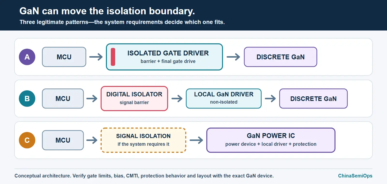
Pattern A uses an isolated driver that matches the GaN device’s gate structure, UVLO, CMTI, isolation class and layout limits. Pattern B moves the final driver close to the gate, while a digital isolator and an isolated bias supply provide the barrier. Pattern C keeps the gate loop and some protection inside the power device and leaves controller-interface isolation to the system design. TI’s LMG1210 is a useful non-isolated local-driver contrast, not an isolated-driver recommendation.
China already has drivers; the harder gaps matter more
Global suppliers already cover smart IGBT/SiC drivers, dual isolated drivers, fast wide-bandgap drivers (drivers for semiconductors such as SiC and GaN, whose bandgap, the energy needed to free an electron to carry current, is wider than silicon’s) and isolated bias. The public product pages of two IC (integrated circuit, or chip) vendors show examples of their stated roles in this category:
- Chipanalog lists the CA-IS3215ENW-Q1 as an active, automotive, single-channel reinforced isolated gate driver.
- 3PEAK describes the TPM23513B on its product page as an isolated gate driver for industrial applications. Its about page gives its headquarters as Suzhou, China.
These are manufacturer statements about their own listings, checked 2026-10-22. They do not show market share, actual availability, qualification in a given system, or any relationship with ChinaSemiOps. For a design in China, as anywhere, the reader still has to confirm the current datasheet, the certificate scope and the supply terms directly with the manufacturer.
In our reading, the harder open work sits in difficult combinations. Examples are fast SiC protection with fewer false trips and controlled turn-off on real modules, regulated isolated bias with monitoring, and useful telemetry without unacceptable latency or software burden. Another is coordination across many floating gate-drive domains (circuits whose reference voltage moves relative to ground) in stacked high-voltage converters. Adaptive drive and programmable slew (a settable rate of voltage change at turn-on and turn-off) also need measured EMI, loss, overshoot and fail-safe results rather than a feature list. These are general design questions, not uniquely Chinese ones.
A practical selection sequence
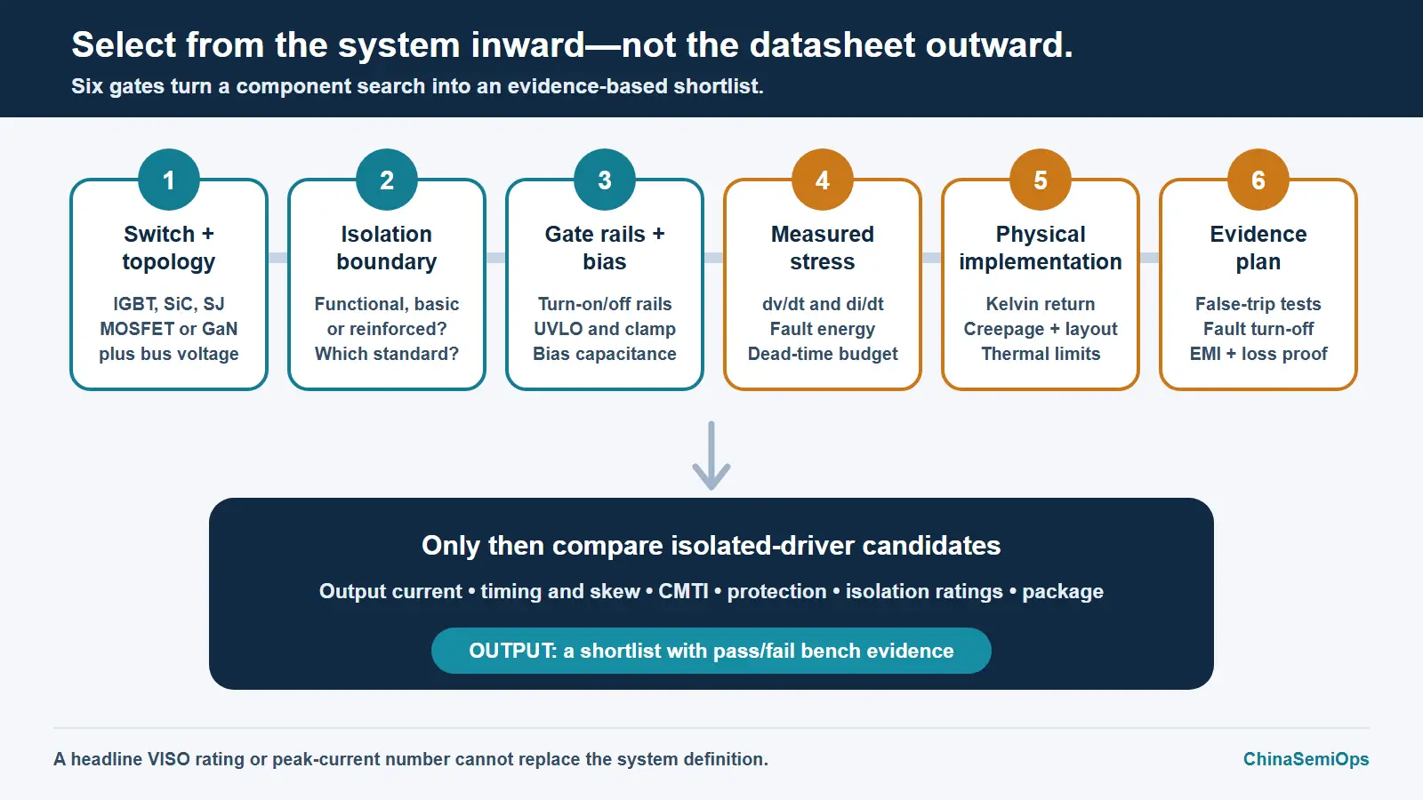
Before opening a driver shortlist, write down six things. The first two define the system and the barrier:
- The exact switch, topology and bus voltage.
- The safety boundary, the working voltage, the end-equipment standard and the waveform and duration behind each isolation rating you will compare.
Items 3 to 6 are design checks. The creepage and clearance in item 5 also belong to the barrier assessment:
- The gate rails, the isolated-bias architecture and the acceptable power-up behavior.
- Target or expected
dv/dt,di/dt, overshoot, fault energy and protection timing, replaced by measured values once a prototype exists. - The package, creepage, clearance and gate-loop layout constraints.
- The bench evidence, the qualification plan and an owner for each remaining risk.
Then compare driver candidates using the same isolation terms and the same pass/fail tests.
Next step: take one candidate datasheet and fill in the ratings table above for it. Write down the waveform, duration and test conditions behind each entry, and list what is missing. Those gaps are the questions to put to the manufacturer.
Selected primary sources
- TI UCC21750 datasheet SLUSD78C (January 2023), section 6.6 — the dated revision used for the worked reading. The current datasheet PDF (portable document format) link is a separate, live link that may point to a later revision.
- TI UCC21750-Q1 — protected isolated gate-driver functions and explicit isolation terms (automotive variant).
- TI Isolation Glossary — definitions of working, repetitive-peak, transient, withstand and surge isolation ratings.
- TI Isolation Glossary SLLA353A (revised September 2017) — working and repetitive-peak voltages as manufacturer-assigned ratings; VISO as a one-minute withstand rating; functional, basic and reinforced insulation. Checked 2026-10-22; not shown to be the latest edition.
- TI SDAA268 (June 2026) — insulation coordination depends on equipment context, working voltages, material group, pollution and altitude.
- TI SSZTDB0 (September 2025) — transformer interwinding capacitance carries common-mode current during switch-node transitions.
- Infineon 600 V CoolMOS P6 application note (revision 1.1, 2015-06-29) — superjunction charge balance (section 1.3, p. 4) and PFC and LLC as listed application examples (section 1.2, table 2, p. 3); a dated foundational example, not a current product or market-frequency claim.
- 3PEAK about page — the manufacturer’s statement of its headquarters location; attributed, no further inference.
- TI UCC21520 — dual-channel isolated-driver architecture.
- Chipanalog CA-IS3215ENW-Q1 — manufacturer listing of an automotive reinforced isolated gate driver.
- 3PEAK TPM23513B — manufacturer listing describing an isolated gate driver for industrial applications.
- TI LMG1210 — non-isolated GaN/MOSFET local-driver contrast.
Related ChinaSemiOps insights
- GaN Gate-Driver IC Opportunities in Robot Joints
- Where Solid-State Transformers Create Real Power-IC Opportunities
- Where HVAC (heating, ventilation and air conditioning) Growth Creates Semiconductor Opportunities
Disclosure: This is a public-source engineering explainer, not a product qualification or component recommendation.