
For 48V AI rack power, the next design question is not only whether distribution moves toward a higher-voltage DC bus. It is where voltage should be reduced between the protected accelerator-board input and the GPU or ASIC rail.
ChinaSemiOps has already examined the wider 48 V-to-800 V AI-factory transition and the 48/54 V board-entry eFuse or hot-swap decision. This Insight starts downstream of both boundaries: at the conversion assembly and power-distribution network serving an accelerator’s very-low-voltage, high-current rail.
Three takeaways
- “Direct-to-chip” is a placement decision, not evidence that 48/54 V enters processor silicon or that one IC performs every power function.
- An intermediate bus can still be the lower-risk option; close-coupled and package-adjacent delivery trade a shorter current path for tighter electrical, thermal and service coupling.
- The most credible IC opportunities sit at a defined boundary: protection, control, sensing, fault capture, telemetry or packaging – not a slogan about a universal AI-rack power IC.
The useful question is therefore not “Is direct-to-chip power better?” It is: for this accelerator platform, does retaining an intermediate bus reduce total risk more effectively than moving a 48/54 V conversion stage close to the load?
Define direct-to-chip before comparing it
Here, direct-to-chip means that a 48/54 V-class distribution rail is converted by an assembly placed unusually close to GPU or ASIC power pins. The assembly may be close-coupled, vertically placed or package-adjacent. It does not mean that 48/54 V enters processor silicon, that a single IC performs every conversion step, or that this arrangement is already a universal production architecture.
OCP’s Open Accelerator Infrastructure UBB specification documents a 48/54 V nominal accelerator-baseboard input context, including a 40.0-59.5 V operating range and dedicated hot-swap control at each OAM input. That establishes a useful board-level boundary; it does not dictate a universal GPU-core conversion topology. OCP OAI UBB Base Specification
Three architectures, one physical problem
All three approaches must deliver a stable low-voltage rail during severe load steps while keeping copper loss, loop inductance, temperature and fault energy inside a validated envelope.
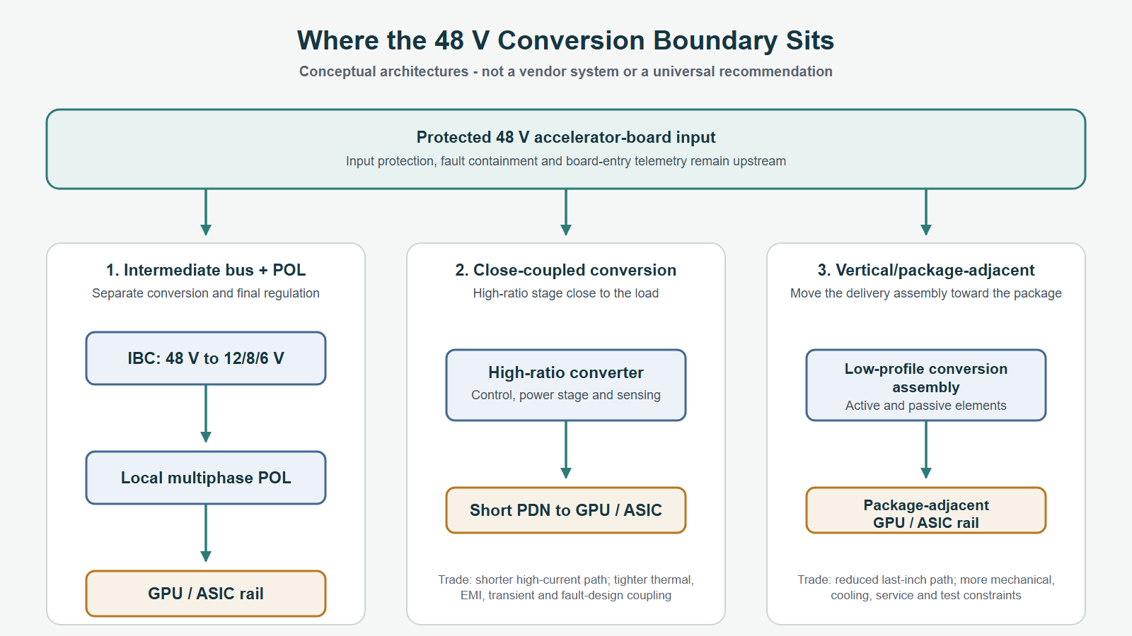
| Architecture | Conversion path | What it optimizes | What becomes harder |
|---|---|---|---|
| Intermediate bus + POL | 48/54 V to IBC, then 12/8/6 V-class rail, then local multiphase regulation | Separates high-ratio conversion, regulation and final load transient into familiar blocks | Two-stage loss and volume; intermediate-rail current and PDN work remain |
| Close-coupled 48/54 V-to-core | A high-ratio converter assembly supplies a core rail near the package | Shortens the high-current path from regulator to load | Conversion ratio, transient response, switching parasitics, sensing and cooling converge in one area |
| Vertical/package-adjacent delivery | Conversion and/or local regulation placed near the opposite side of the package or board | Can reduce the last-inch current path and free board routing | Mechanical stack-up, cold-plate clearance, serviceability, EMI and test access become core constraints |
OCP’s 48 V onboard-power work describes first-stage requirements including fixed-ratio conversion options, protection, monitoring and telemetry. That supports the continuing relevance of an intermediate-bus architecture; it does not make it obsolete. OCP 48 V Onboard Power Solution Requirements
As a vendor example of that retained boundary, Infineon describes 48 V intermediate-bus converters feeding separate downstream point-of-load regulators for XPUs and AI ASICs. This is an attributed vendor architecture example, not an independently validated performance comparison. Infineon: Intermediate bus converters in AI data centers
Renesas describes 48 V-to-core conversion as a more direct approach alongside intermediate and vertical-delivery paths. Its paper identifies efficiency, current-density and transient behavior as design targets, rather than declaring a single industry winner. Renesas, Power Architecture Evolution in Data Centers
Why distance from the accelerator matters – and does not settle the answer
At low load voltage, the current needed for a given power rises. Long copper paths between regulator and processor can consume voltage margin and add impedance to the PDN. Vicor uses this constraint to motivate placing regulation close to CPU, GPU and AI-processor load pins. That is useful topology vocabulary, but it remains a vendor architecture statement – not proof that one placement wins in every rack. Vicor, Factorized Power Architecture
Moving the converter closer to the load changes rather than removes the problem:
- A shorter output-current path may improve the local PDN, but the switching loop still needs low inductance and controlled EMI.
- A large 48/54 V-to-core ratio and a fast accelerator load transient must be handled together, not optimized separately.
- Heat from switches, magnetics, capacitors and interconnects becomes more concentrated near the package and cooling hardware.
- A compact module can reduce footprint yet make assembly, inspection, rework and fault replacement more consequential.
GaN is an option; monolithic is a different claim
GaN can be valuable in selected high-frequency or high-voltage switching stages. But GaN, an integrated half-bridge, a multi-die power module and a monolithic converter IC are different things.
TI’s LMG5200POL evaluation module documents one technical path: a 36-54.5 V input converted to 0.5-1.5 V at up to 50 A using an 80 V GaN half-bridge power stage with an integrated gate driver and a separate controller. It demonstrates that a 48 V-class GaN point-of-load path can be built and evaluated. It is not evidence of a production GPU rail, a complete AI-rack topology or a monolithic 48/54 V-to-core converter. TI LMG5200POLEVM-10
This is the right discipline for a direct-to-chip discussion. Do not combine an unverified rack-power number, a topology, an alleged deployment and monolithic integration into one headline claim. Each needs its own primary evidence.
The IC partition moves with the conversion boundary
ChinaSemiOps engineering inference: the following design consequences depend on the actual converter, PDN, package and cooling implementation. As the conversion assembly approaches the accelerator, five functions become more tightly coupled.
1. Controller and power-stage coordination
A fixed-ratio front element can ease the final regulation task. A tightly regulated high-ratio stage can remove a boundary but raises control-bandwidth and fault-coordination demands. The relevant comparison is the complete transient, loss and validation budget – not a peak-efficiency headline.
2. Fast protection versus fleet telemetry
OCP’s first-stage requirements explicitly include over-current, short-circuit, voltage, power and temperature protection, plus monitoring and fault/status information. OCP 48 V Onboard Power Solution Requirements
ChinaSemiOps engineering inference: fast local protection needs a deterministic hardware path, while supervisory telemetry supports BMC policy, diagnostics and derating. A management interface should report a fault; it should not be the only mechanism expected to stop one.
3. High-bandwidth sensing and event capture
At a close-coupled boundary, current and voltage measurement must distinguish normal load excursions from an unsafe condition. A credible IC opportunity may therefore be a protected controller or analog front end with calibrated sensing, fast fault capture and useful event history – not necessarily a universal all-in-one power IC.
4. Gate drive and layout as one design problem
An integrated driver/power-stage approach can simplify a critical gate loop. However, exact voltage stress, dv/dt, dead time, short-circuit response, layout parasitics and thermal limit remain platform-specific validation work. Integration alone is not a product moat.
5. Package, thermal and service co-design
At high current, the limiting path may be an interconnect, capacitor, inductor or cold-plate interface rather than the controller die. First architecture reviews should ask:
- Where is heat removed: through a cold plate, board, baseplate or multiple paths?
- Is the sensed temperature representative of the actual limiting element?
- Can phases share current symmetrically through the intended stack-up?
- Does the module leave realistic access for assembly, test, debug and replacement?
- Does high-frequency power placement compromise high-speed signal routing?
A decision screen before choosing an IC program
| Question | Why it decides the architecture |
|---|---|
| What are the real input range, surge and fault cases? | Defines voltage rating, protection and safe-operating-area work; nominal “48 V” is not enough. |
| What must the load transient look like at package pins? | Determines PDN, local energy storage, control bandwidth and placement. |
| Is the high-current path or conversion ratio the harder constraint? | Helps decide whether an intermediate bus retains useful separation. |
| Who owns cooling, module assembly, test and replacement? | Determines whether a package-adjacent module is practical or creates an unserviceable boundary. |
| Which measurement and fault data must reach the BMC? | Defines the telemetry controller opportunity without replacing the autonomous protection path. |
ChinaSemiOps view: own a hard interface, not a slogan
The attractive opportunity is not “a GaN IC for every AI rack.” It is a verified interface at a specific conversion boundary: protected high-ratio control, high-bandwidth sensing, fault/event capture, module telemetry, or a package and interconnect implementation that measurably improves a defined platform’s PDN and thermal envelope.
The intermediate bus can remain the lower-risk answer. Close-coupled or vertical delivery can become compelling when the last-inch current path truly dominates. Neither conclusion should be made from a voltage label, a single module demonstration or a vendor roadmap alone.
Before a custom IC starts, define the input/fault envelope, target conversion boundary, package/cooling stack-up, transient requirement, measurement accuracy, service model and qualification ownership. That turns direct-to-chip from a headline into an engineering decision.
Selected public sources
- OCP OAI UBB Base Specification r2.0
- OCP 48 V Onboard Power Solution Requirements
- Renesas: Power Architecture Evolution in Data Centers
- TI: LMG5200 48 V-to-1 V GaN POL evaluation module
- Vicor: Factorized Power Architecture
- Infineon: Intermediate bus converters in AI data centers
Working on a 48/54 V accelerator power path? Start by mapping the input and fault envelope, conversion boundary, PDN target, thermal stack-up and service model before selecting an IC partition. For public-source research and architecture discussion, contact ChinaSemiOps.