Consider a hypothetical case. A pilot-run power converter stops switching. Its protection tripped, one power transistor now measures as a short circuit, and a technician notices a dark mark near the package edge. The manager asks: do we send it out to be cut open this week?
That is the everyday decision behind failure analysis of silicon carbide (SiC) and gallium nitride (GaN) power devices, the work of finding out why a power device failed. SiC and GaN are two semiconductor materials used for power switches. Whatever the material, a cut cannot be undone, and the dark mark may or may not be where the failure started.
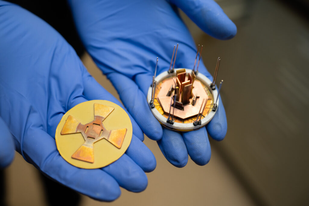
Silicon-carbide power module, photographed May 2, 2025. Representative power-electronics hardware, not a failed sample. Photo: Brooke Buchan, National Laboratory of the Rockies (NLR)/U.S. Department of Energy, image 100033. Source · Image-use terms.
Key takeaways
- Visible damage is a symptom. The first event may be somewhere else.
- Record the history and keep the sample as received before any cleaning, powering or cutting.
- Choose each analysis method by the question it can answer, and ask the lab about its limits.
- Agree on a hold point before any irreversible step, such as opening the package (removing part of the casing to expose the chip) or cutting. Cutting can be skipped.
- Keep SiC and GaN hypotheses separate. Do not borrow one material’s structure for the other.
Five-stage evidence workflow for a failed power device
- Preserve. Record the history and identifiers. Keep the sample as received.
- Localize. Choose a compatible method that can locate the anomaly, non-destructive where feasible. If localizing needs an irreversible step, such as opening the package, take it to the hold point first.
- Agree a hold point. Before any irreversible step, decide with the lab whether opening the package or cutting would add information. If cutting would not, skip stage 4 and go to stage 5.
- Section only if justified (optional). Make a targeted cut only after that agreement.
- Correlate and verify. Combine the evidence, then check that the corrective action fits the mechanism.
Bypass: stage 4 is optional. If the hold point concludes that cutting adds nothing, skip stage 4 and go directly from stage 3 to stage 5.
Preserve the evidence before changing the sample
Start with paper, not tools. Write down the part number, revision and lot, the package type, and the exact device technology from the datasheet. Add the timeline: what the converter was doing, which protection events were logged, what changed recently, and whether anyone has already measured, cleaned or reworked the part.
Photograph the sample as received, label its orientation, and store it so nothing touches the damaged area. Do not re-power a failed converter to “see what happens.” Plan any electrical measurement with the analysis lab first, and ask whether the measurement could change the damaged sample.
An 8 October 2026 Power Electronics News interview on power-device failures carries a warning that cutting a chip open to prepare it can destroy the very feature you wanted to examine. That is one interviewee’s warning, not an independent study. It is the reason this article proposes a hold point before preparation steps.
Keep SiC and GaN failure hypotheses separate
SiC. Before choosing any test, write down the exact part, and establish its device architecture with the lab and the datasheet. Then ask history questions. Has the gate terminal seen unusual stress? Which current paths were recorded? Was there a short-circuit event? Is there package damage? Each answer points to a different next check, and none is a conclusion by itself.
GaN. Texas Instruments’ 2021 technical report on GaN failure mechanisms (SNOAA68) is a vendor document. It says: “Charge can be trapped in the buffer layer, in dielectrics, and at interfaces.” Texas Instruments therefore advises evaluating dynamic on-state resistance, the resistance while conducting shortly after switching stress, at the timescales of switching cycles. When you brief the lab, ask how soon after the stress the resistance was measured, under what temperature and contact conditions, and how they would interpret a higher reading. Texas Instruments’ product-specific lifetime figures are not used here.
Record the exact architecture of the part. Keep SiC and GaN hypotheses separate, and confirm the actual part’s structure with the lab and the datasheet.
Match the analysis method to the question
Where feasible, start with methods that leave the sample unaltered, and ask the lab whether each method carries any risk to it. The table is our proposed planning aid, not a lab procedure and not a list of source-established limits; its third column is questions to put to the lab. Fraunhofer’s institute page on failure analysis (linked in the sources below) lists acoustic investigation, lock-in defect localization, scanning electron microscopy with elemental analysis, and sample sectioning by sawing, grinding and polishing. ZEISS’s application page (also linked below) shows example images of specific samples, such as a cleaved (split open) silicon carbide device, a thin slice of gallium nitride, and a virtual section through connections in a power-management chip. A listing or vendor example shows that a method exists. It does not show that a lab can run it on your sample today, or that the method will prove a cause, so confirm both with the lab.
| Method | Question it can help answer | Question to ask the lab |
|---|---|---|
| Records and visual inspection | Which sample, terminals and regions visibly changed? | Which visible changes should be documented before anything else is done? |
| Electrical characterization: current–voltage curves (how current responds to voltage), gate leakage (unintended current at the gate terminal under stated conditions) | Which parameter changed, and under what temperature, timing and prior stress? | Which timing, temperature and contact conditions apply, and how would you interpret a changed value? A change alone does not name the mechanism. |
| Scanning acoustic microscopy: uses sound to look for voids, cracks or layers separating | Is an interface suspect? | Can this package be examined this way, and what would a finding not tell us? |
| Lock-in thermography: a defect-localization method listed by the institute | Where does an anomaly sit? | Who applies any electrical stimulus, and under what conditions? Never re-energize a failed converter yourself. |
| Scanning electron microscopy (SEM) with energy-dispersive X-ray spectroscopy (EDS): magnified imaging plus elemental analysis | What shape and which elements are at a region? | Does this need the package opened or the part sectioned first? If so, take that step to the hold point. An element signal alone does not establish origin, timing or supplier fault. |
| Sectioning by sawing, grinding and polishing | Would a section answer a question the earlier evidence cannot? | Irreversible. Is this step needed at all, what target is agreed, and what is recorded before and after? |
Agree on the hold point before opening or sectioning
A hold point is a deliberate pause before an irreversible step, such as opening the package or cutting. The sample owner and the analysis lab review what is known and answer a few questions. What would opening the package or cutting reveal that the earlier evidence cannot? Where would the opening or cut go, and in what orientation? Which records are kept, what material remains, and what result would make you stop?
If locating the anomaly seems to require opening the package, bring that step to the hold point first, even though it feels like part of localization. This is our planning recommendation, not a requirement stated by the sources.
Sometimes the honest answer is that cutting adds nothing, because non-destructive evidence already separates the explanations. Then skip it. Sometimes localization is too vague to aim a cut. Then preserve the sample and report the uncertainty.
Sample-handoff checklist (general; useful wherever the analysis is done):
- Exact part identifiers, package and device technology.
- Chronological operating and failure history, including protection events.
- Existing electrical records, with conditions, timing and temperature.
- As-received photos, handling record, and comparison samples if available.
- Your hypotheses and the next question that would separate them.
- The proposed irreversible step (opening the package or cutting), its target and orientation, and who agrees to it.
- What you will keep, and what would make you stop.
Turn correlated findings into a corrective-action plan
Line up the evidence: where the electrical anomaly sits, what the physical observations show, what stress the part saw, and what the comparison samples look like. An analysis image can show where damage is; it does not by itself show what started it. Then sort each finding. Is it the initiating mechanism, damage that followed, or a change introduced by sample preparation? Ask the lab how it would tell these apart for each finding.
List the explanations still consistent with the evidence. A corrective action should address the mechanism you can support, and its effect should be verified under a relevant qualified test plan. One image does not prove supplier fault, and no analysis promises that a failure will never recur.
Back to the converter: the next step is not “cut it this week.” It is to prepare the handoff above and ask which result would separate the competing explanations.
Selected sources
- Fraunhofer Institute for Integrated Systems and Device Technology, Failure Analysis (institute method listing; revision date not shown; read 22 Oct 2026).
- ZEISS, semiconductor application page (analog, radio-frequency, power, micro-electromechanical and sensor devices; vendor examples on specific samples; revision date not shown; read 22 Oct 2026).
- Texas Instruments SNOAA68, Addressing GaN Failure Mechanisms (vendor technical report, 2021; read 22 Oct 2026; whether a newer revision exists was not verified).
- Power Electronics News, interview on finding the root cause of power-device failures (8 October 2026; one interviewee’s warning, not an independent study).
Please link to this article when sharing. Contact us for permission to republish the full article.