
Electric-vehicle charging is one application for power semiconductors. This photograph illustrates the application only; it does not identify the semiconductor technology or wafer size inside this charger. The photograph is licensed under Creative Commons Attribution–ShareAlike 4.0 (CC BY-SA 4.0): credit the creator and use the same or a compatible license for shared adaptations of the photo. Photo: Matti Blume / Wikimedia Commons, July 4, 2026, CC BY-SA 4.0.
Suppose the supplier of a silicon carbide (SiC) power device you buy tells you it is moving production from 150 mm to 200 mm wafers. A wafer is the thin round slice of crystal on which many chips are made, and the number is its diameter. SiC is a compound semiconductor used to make devices that switch high voltages efficiently, which is why it appears in electric-vehicle (EV) chargers and other power equipment. Does a 200 mm SiC wafer mean a lower cost per device, and what should you ask for before you believe it?
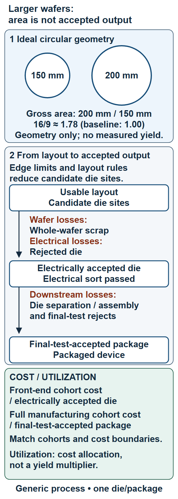
The short answer: not automatically. A 200 mm wafer has about 1.78 times the circular area of a 150 mm wafer, but you buy accepted devices, not area. Whether the cost per accepted device falls depends on how many dies (the individual chips cut from a wafer) survive layout, wafer losses, electrical testing, packaging and final test, and on how the supplier counts its cost.
Three takeaways
- Larger area is a geometric fact. Lower cost per accepted device is a claim that needs product-specific evidence.
- Compare costs only for the same wafers, with the same cost boundary and the same denominator (the number you divide by), preferably accepted dies.
- A supplier's wafer-size announcement is not your customer release for your part.
A larger wafer provides area, not a device-cost promise
Fact (geometry): circle area scales with the square of the diameter, so 200² ÷ 150² = 16/9, or about 1.78. That is 77.8% more gross area, not 77.8% more good devices.
Some of that area is unusable. A die is one individual chip cut from the wafer. The layout leaves out an edge exclusion ring around the rim, the small flat edge or notch that marks the crystal direction, the narrow saw lanes (scribe lanes) between dies, and space for test patterns. Gross die means the complete die sites that fit this layout, before any electrical judgment.
Geometry at 16/9 does not by itself establish a price or an accepted-die gain.
Count accepted die before comparing front-end cost
Front-end cost means everything spent to make the wafer and bring it through electrical sort, which is the test of each die on the wafer. It includes the substrate (the SiC wafer you start with), epitaxy, fabrication, measurement and sort, and it includes wafers that were later scrapped. Epitaxy is the growth of a thin crystal layer on the substrate, where the device is built.
Use these terms consistently:
- Wafer survival: wafers that reach electrical sort, divided by wafers started.
- Electrical yield: accepted dies divided by the dies tested. State which dies are counted, and whether whole-wafer losses are already included, so they are not counted twice.
- Accepted die: a die that passes electrical sort.
Pick one cohort, meaning a group of wafers started together and followed through the same steps, and keep numerator and denominator on the same wafers. Either divide the cohort's front-end cost by its accepted dies, or compare the average front-end cost per wafer started with accepted dies per wafer started. Do not divide the cost of a processed or surviving wafer by output counted per started wafer, or the reverse.
Break-even then follows directly: the 200 mm average cost per wafer started may rise only as much as accepted dies per wafer started rise.
Hypothetical example. Every input is invented. Units are arbitrary, not currency, and no vendor data is used:
| Measure | Invented 150 mm case | Invented 200 mm case |
|---|---|---|
| Wafers started | 100 | 100 |
| Wafer survival | 0.95 | 0.90 |
| Gross die per surviving wafer | 100 | 170 |
| Electrical yield | 0.90 | 0.75 |
| Accepted die per wafer started | 85.5 | 114.75 |
| Front-end cost per wafer started (units) | 1.00 | 1.60 |
| Cohort front-end cost (units) | 100 | 160 |
| Cohort accepted die | 8,550 | 11,475 |
| Cost per accepted die | 0.0117 | 0.0139 |
Here accepted dies per wafer started rise about 34%, but cost per wafer started rises 60%, so cost per accepted die is about 19% higher. Break-even would need the 200 mm cost per wafer started to stay at or below about 1.34 units. Change the invented inputs and the answer can reverse. The lesson is the method, not the numbers.
Follow scrap, utilization and packaging as production grows
Ramp-up is the period when a factory raises output from first production toward planned volume. Accepted dies are not shipped devices. After sort, dies are cut apart, assembled into packages and tested again. Each step has its own losses and costs. A full comparison asks for cost per final-test-accepted packaged device, and states whether depreciation, ramp engineering, overhead and warranty are included. A module that holds several dies needs a calculation based on its bill of materials (the list of dies and other parts), using each part's yield and cost, rather than one package yield. Packaging and test losses are separate from wafer electrical yield, so ask for them separately.
Utilization is how much of a factory's declared capacity is actually used. It belongs on the cost side: fixed costs spread over fewer wafers raise cost per wafer. It is not an electrical yield, and accepted dies should not be multiplied by it.
Vendor statement: STMicroelectronics (ST) files Form 6-K reports with the US securities regulator. Its Form 6-K for the second quarter of 2026 reports charges for unused capacity at company level. That shows unused capacity is a real cost line, but it is not a SiC-only or ramp-specific figure and it gives you no number for your part.
Material quality is also something you can ask about. Vendor statement: Wolfspeed's September 27, 2026 release for a premium 200 mm substrate attributes the improvement to defect metrics and wafer-shape consistency. AIXTRON's G10-SiC product page lists 150 mm and 200 mm epitaxy configurations, including batches of nine 150 mm or six 200 mm wafers. The Fraunhofer Institute for Integrated Systems and Device Technology (IISB), a research institute, describes full-wafer measurement and linking substrate and epitaxial-layer properties to electrical device results. Inference: these are reasons to ask for data, not evidence of your part's yield. A defect count alone does not tell you how many dies will fail, and a batch size alone does not tell you cost without cycle time, recipe (the process settings) and accepted output.
Separate a China-based manufacturing milestone from customer access
Qualification is documented proof against stated requirements. The following China example provides supporting context. Vendor statement (dated): in its Form 6-K for the quarter ended June 27, 2026, ST describes a joint venture (JV) in Chongqing for 200 mm SiC devices made exclusively for ST using ST technology, a separate substrate facility that Sanan Optoelectronics, ST's partner in the Chongqing venture, is planning to build, and ST's second-quarter statement on production readiness and ramp-up.
Read this as a statement about the second quarter and about plans, not as measured October output or yield. A location is not an open foundry service (manufacturing chips for other companies), a qualification or an allocation for you. ST has announced that it will release its third-quarter 2026 results on October 29, 2026, after this article's evidence date of October 27, 2026, so check the latest company disclosure before relying on this paragraph. The same caution applies to any supplier, in any country.
Fact (background): On October 15, 2026, Infineon and Wolfspeed announced a multi-year agreement covering 200 mm SiC wafers (Wolfspeed, Infineon). That concerns upstream material. It does not establish the delivered volume, price or qualification status of your finished part.
Ask suppliers for evidence at each release boundary
Customer release is your approval for your product and production. A supplier's process or device qualification does not replace your approval to use the part in your product. For the broader transfer checklist, see When a Power or Analog Process Moves Fabs, What Must Be Re-Proven?. The table below covers only what changes with diameter and applies to any supplier.
| Question | Evidence to request | It does not show |
|---|---|---|
| Which parts, ratings and packages does the 200 mm offer cover? | Part-level scope and change notice | Other parts |
| How is gross die count defined? | Layout, edge exclusion, saw lanes | Accepted die |
| What do survival and yield cover? | Cohort, test limits, denominators | Package yield |
| How are ramp, scrap and utilization handled? | Cost boundary and what is excluded | Selling price |
| What do packaging and final test lose? | Per-stage losses and costs | Wafer yield |
| What approvals exist for your part? | Dated material, device and customer-release records | Allocation |
Next action: send these six questions in writing and keep the answers in three separate files: material evidence, device evidence and customer-release evidence.
Primary sources (accessed October 27, 2026)
- Wolfspeed: Infineon and Wolfspeed expand and extend long-term SiC wafer supply agreement to include 200 mm (October 15, 2026)
- Infineon press release on the expanded Wolfspeed agreement (October 2026)
- STMicroelectronics (ST) Form 6-K for the quarter ended June 27, 2026: Chongqing JV, Sanan substrate facility plan, devices made for ST, ramp-up, unused-capacity charges
- ST: timing of third-quarter 2026 earnings release and conference call
- Wolfspeed: new premium 200 mm SiC power substrates (September 27, 2026)
- AIXTRON G10-SiC product page (undated)
- Fraunhofer Institute for Integrated Systems and Device Technology (IISB): silicon carbide materials (undated page)
Please link to this article when sharing. Contact us for permission to republish the full article.