Suppose three jobs each need an artificial intelligence (AI) chip: a speech model on a small local, or edge, device; fine-tuning a language model at a desk, which adapts a trained model with new data; and training (teaching a model from data) plus inference (using a trained model to answer requests) in a data center. These hypothetical jobs have different AI workloads.
Five labels dominate the conversation: CPU (central processing unit, the general-purpose processor), GPU (graphics processing unit, a processor for graphics and parallel computing), NPU (neural processing unit, a processor or block for neural-network work), LPU (language processing unit, an inference architecture associated with Groq) and TPU (tensor processing unit, Google’s accelerator family; a tensor is a multi-dimensional array of numbers). Start with the workload, then map the system around it.
Three takeaways
- The labels overlap: CPU, GPU and NPU name broad processor functions; LPU and TPU are associated with specific vendors’ architectures.
- Software support, memory and data movement shape fit more than a label does.
- Chip design, manufacturing, packaging, testing and system integration are separate responsibilities.
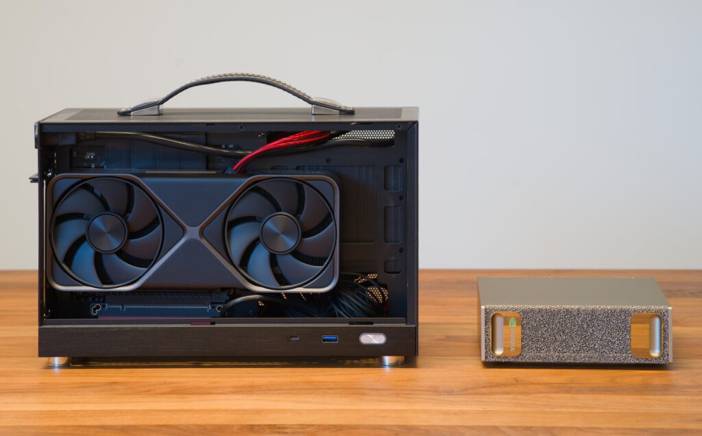
Featured photo: small-form-factor desktop computer with a GeForce RTX 5070 next to an NVIDIA DGX Spark by Daniel Lu (dllu), May 16, 2026, via Wikimedia Commons, CC BY-SA 4.0 (Creative Commons Attribution-ShareAlike: reuse requires credit, and adaptations must use the same or a compatible license; this license covers the photo only, separately from the article-reuse notice below). Image resized.
Start with the model, software and operating conditions
A voice assistant on a local device cares about latency, the delay before an answer arrives, measured to the first output or to the complete response. A shared serving cluster cares about throughput, total work finished per second, and concurrency, how many requests are active at once. For language models, a token is a small chunk of text, context is how many tokens the model keeps in view, and a batch is a group of requests processed together.
An operator is one building-block calculation in a model; a compiler is the software that translates the model into instructions for a processor; a runtime is the software that executes it. Before comparing devices, match model, runtime, operator support, quality target, batch, context, concurrency and data movement, and the latency or throughput you need.
Five processor labels and where their roles overlap
| Label | What it names | Documented example | Check first |
|---|---|---|---|
| CPU | General-purpose processor | Google’s guidance lists CPUs for flexible prototyping and small models or batches | Does your runtime support the model on this CPU at your batch size? CPUs also train and infer. |
| GPU | Processor for graphics and other parallel computing; in NVIDIA’s CUDA (Compute Unified Device Architecture, its GPU-programming platform), a device the CPU host controls | The CUDA guide describes the host-and-device pattern | Do your framework (model-building software library) and CUDA version cover the model’s operators for training or inference? How much data copies between CPU and GPU memory? |
| NPU | Processor or block for neural-network work | Arm markets Ethos-U85 as edge NPU IP (intellectual property, a reusable circuit design) supporting transformer models, a neural-network design used for language and vision models | Does the compiler accept every operator? What falls back to the CPU? |
| LPU | Inference architecture associated with Groq | Groq’s March 2025 article describes compiler-scheduled compute and data movement with on-chip SRAM (static random-access memory, fast on-chip memory) | Which generation and compiler does your model target? |
| TPU | Google’s accelerator family | TPU7x documentation covers training and inference with JAX and PyTorch frameworks; TensorFlow is unsupported | Is your framework supported, and does the model fit? |
Check compiler and operator support before peak arithmetic rates
Arm’s Vela compiler takes a quantized model (reduced to low-precision integers) in TensorFlow Lite (TFLite, a compact edge model format) or TOSA (Tensor Operator Set Architecture, a standard set of basic tensor operations) form and generates commands for an Ethos NPU. With TFLite, operators the NPU cannot run stay on the CPU; the documentation states that TOSA compilation has no CPU fallback. List which operators fall back: that work runs on another processor, and data must move between them.
Three system examples show where boundaries fall
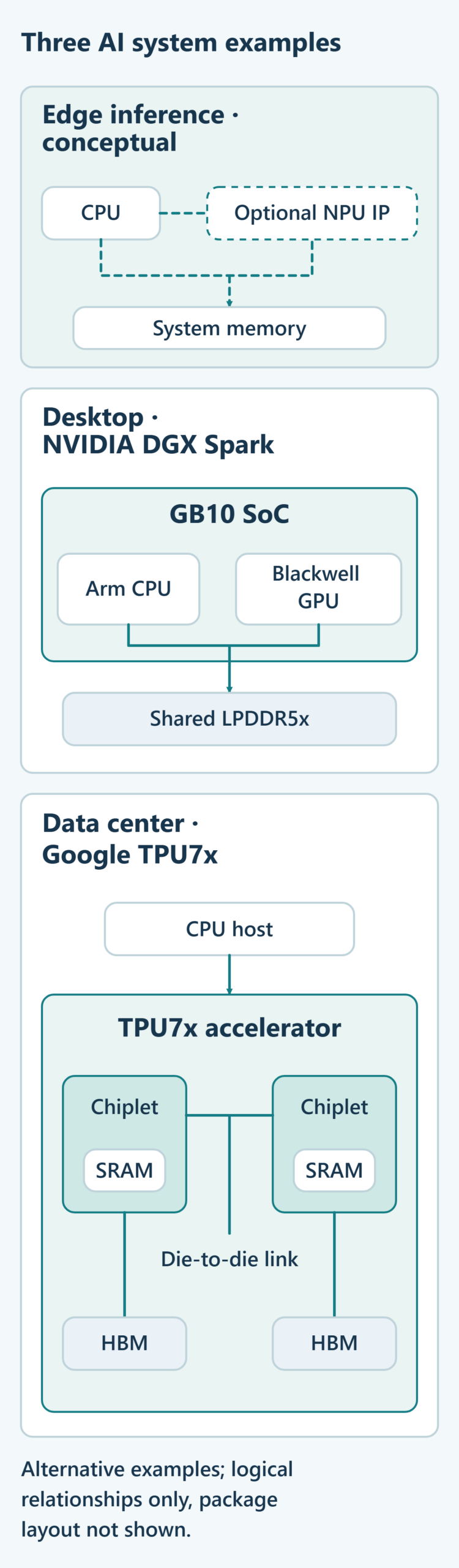
An SoC (system on chip) combines a processor and other functions in one chip design. A die is one piece of silicon cut from a wafer, the thin disc chips are made on; a chiplet is a die designed to work with others; a package connects dies to the board.
- Edge inference: Arm’s Corstone-320 reference subsystem (a vendor’s example design for customers to adapt) integrates a Cortex-M85 CPU with Ethos-U85. A licensed block or reference subsystem is not a customer’s finished SoC, die or package.
- Desktop prototyping: In NVIDIA’s DGX Spark, the GB10 SoC integrates an Arm CPU and a Blackwell GPU sharing LPDDR5x (low-power double data rate 5x, a low-power memory standard). Sharing avoids some duplicate CPU and GPU copies of shared data, but the release notes document display-reserved memory (memory set aside for display output), so usable capacity is reduced and data still moves through memory.
- Data-center training and inference: Google’s TPU7x documentation describes two chiplets, each with its own HBM (high-bandwidth memory, a stacked memory type for very high data rates) memory space, joined by a die-to-die interface (a direct link between two dies); on-chip SRAM serves as fast scratch memory. One example, not a universal layout.
Who designs, manufactures, packages, tests and integrates
Fabless is a business model in which a company designs integrated circuits (ICs, semiconductor chips containing interconnected electronic components) and relies on external wafer fabrication; a foundry manufactures customer designs, as TSMC’s 2025 annual report explains. Processor labels describe functions or vendor architectures, not this business model.
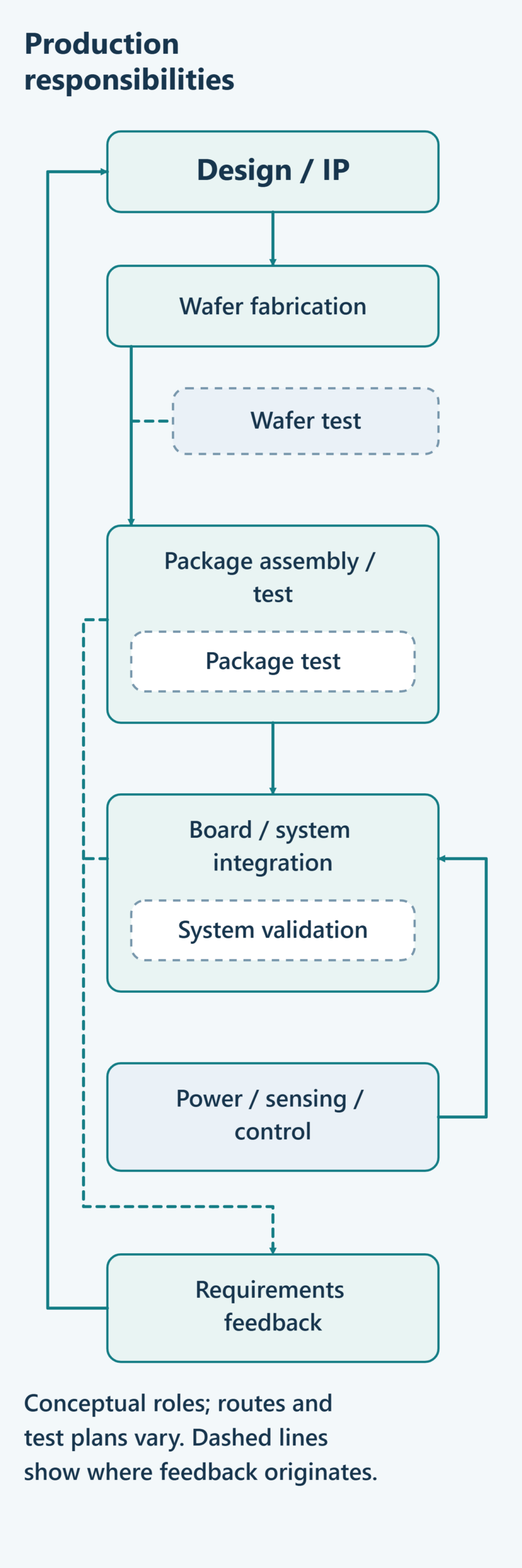
Wafer test, package test and board or system validation are distinct checkpoints. Power conversion (turning the supply into the voltages a chip needs), sensing (measuring voltage, current or temperature) and control form a separate requirement path, and memory, package, thermal and test needs feed back to design. A chip’s thermal design power (TDP, the heat a vendor designs the cooling to handle; a design target, not measured or peak draw), a supply’s rating and measured system consumption are different quantities.
A packaging and test example from China, plus a general checklist
JCET Group, a China-based company, illustrates the packaging and test role. Its website (undated, accessed October 14, 2026) describes turnkey services (one supplier handling the steps end to end) covering wafer bumping (forming connection contacts), wafer probing (electrical testing before cutting the wafer), multi-die assembly and final test. Its August 20, 2026 first-half (H1) disclosure describes AI-related heterogeneous integration, meaning different dies combined in one package. These are JCET’s own statements about company roles; they establish no accelerator-specific qualification, customer relationship or capacity.
This checklist is generally applicable, not uniquely Chinese. For any supplier or design claim, ask:
- Which stage does the evidence cover: wafer, package, board or system?
- Who states it, on what date: vendor statement or measurement?
- Which memory, package, thermal or test limits go back to design?
- Where is the supplier’s own documentation of the exact package type and test steps, with dates?
Five questions for a matched workload comparison
- Which model, framework and runtime version must run, and does each processor path support every operator?
- What batch size, context length and concurrency does the real use case need?
- How much data moves between processors, and where does it sit: shared memory, separate memory spaces, on-chip SRAM or HBM?
- Which matters: the wait for the first output, the wait for the complete response, or throughput for many requests, and at what quality target?
- Which responsibilities fall to design, foundry, package and test, and system integration, and what dated evidence covers each?
Next action: run the same task and data on each candidate under recorded conditions (precision, quality target, batch, context); compiled model files may differ, so compare only matched, recorded results.
Related reading
48 V to the AI Core: Where the Conversion Boundary Becomes the IC Problem and AI Data-Center Liquid Cooling: The Analog ICs Behind Reliable Operation.
Selected primary sources
- Google Cloud, TPU7x documentation, revised October 9, 2026.
- NVIDIA, CUDA Programming Guide, v13.4.2, September 10, 2026.
- Arm, Ethos-U85 product page, undated, accessed October 14, 2026.
- Arm, Vela compiler documentation, undated, accessed October 14, 2026.
- Groq, What is a Language Processing Unit?, March 7, 2025.
- NVIDIA, DGX Spark hardware overview, September 10, 2026.
- JCET Group, company website, undated, accessed October 14, 2026.
- JCET Group, H1 2026 disclosure, August 20, 2026.
Please link to this article when sharing. Contact us for permission to republish the full article.