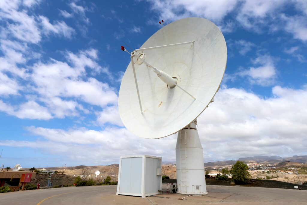
A satellite ground station has a simple job on paper: pull a very weak signal out of noise. Its receive chain, the parts that carry the signal from the antenna toward the receiver, needs gain without much added noise, so the radio frequency (RF) behavior of its amplifiers matters more than their package label. Packaging comes after you know the function, band (frequency range), heat and environment.
Three takeaways
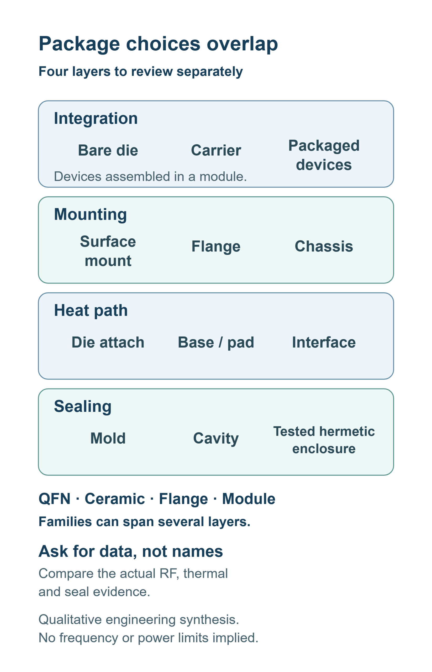
- Integration (devices assembled together in one module), mounting (how a part is attached: soldered flat to a board, or fastened to a chassis, the supporting frame or base, or to a heat sink, a metal structure that sheds heat), heat path and sealing are separate, overlapping layers. A bare die (unpackaged chip), a QFN (quad flat no-lead, a leadless package soldered flat to the board) and a flanged housing (with a metal mounting base) answer different questions.
- High frequency does not automatically exclude a QFN, and a ceramic or metal housing does not by itself show a hermetic seal (one that limits gas and moisture exchange, shown by a leak test). Ask for measured data.
- For depletion-mode amplifiers (normally on: the transistor conducts unless its gate, the control terminal, is made negative enough) made with gallium nitride (GaN), a compound semiconductor of gallium and nitrogen, the device is off only when the gate is at or more negative than its pinch-off (cutoff) voltage, within the datasheet’s gate-voltage limits; a less negative gate may still conduct. The bias order (the sequence in which the steady direct-current, DC, voltages that set the operating point are applied) and the heat path are reviewed together.
Cover photo: ground-station antenna, Maspalomas, Gran Canaria, March 2026. Photo: Rvr, via Wikimedia Commons, CC BY 4.0. It shows application context only, not the system’s band, power, package or transistor technology.
Start from the function, not the package name
Write down what the module must do at its reference plane, the point where RF performance is specified, such as a connector: gain, noise, output power, isolation (leakage between signal paths), band. Then separate four questions that package names blur: how devices are integrated in one module (assembled together, not semiconductor-process integration), how the part is mounted and attached, how heat leaves, and how it is sealed.
Mounting is the physical attachment. Surface-mount technology (SMT) solders a part flat onto a board. A flanged part is fastened to a chassis or heat sink instead. Heat then crosses a thermal interface, the contact or joining layer between two heat-conducting surfaces, from the part’s base or exposed pad (the heat-conducting underside of the package) into what it sits on.
In the map below, a carrier is a small substrate that holds a bare die, mold is plastic molded around the die, a cavity is an air space left above the circuit, and the Interface box is the thermal interface.
Bare die and carriers: flexible, but you own the assembly
A bare die is a chip with no package. Many RF circuits are monolithic microwave integrated circuits (MMICs), a complete RF circuit on one piece of semiconductor such as gallium arsenide (GaAs) or GaN. Attaching the die directly and linking it with short wire bonds (fine metal wires from chip to substrate) gives designers control over the RF transitions (the connections the signal crosses between chip, package and board) and the layout. That design control is our engineering reasoning, not a vendor claim. The Mini-Circuits article discusses the other side: it describes bare-die assembly as manually intensive, notes that a die on a carrier has limited protection, and discusses optimizing the package and its interconnect (the wiring between chip and package).
The cost is responsibility: the module maker owns die handling, die attach (fixing the chip down), bond quality, protection and the thermal path to the housing. More design control does not mean inherently best or fastest.
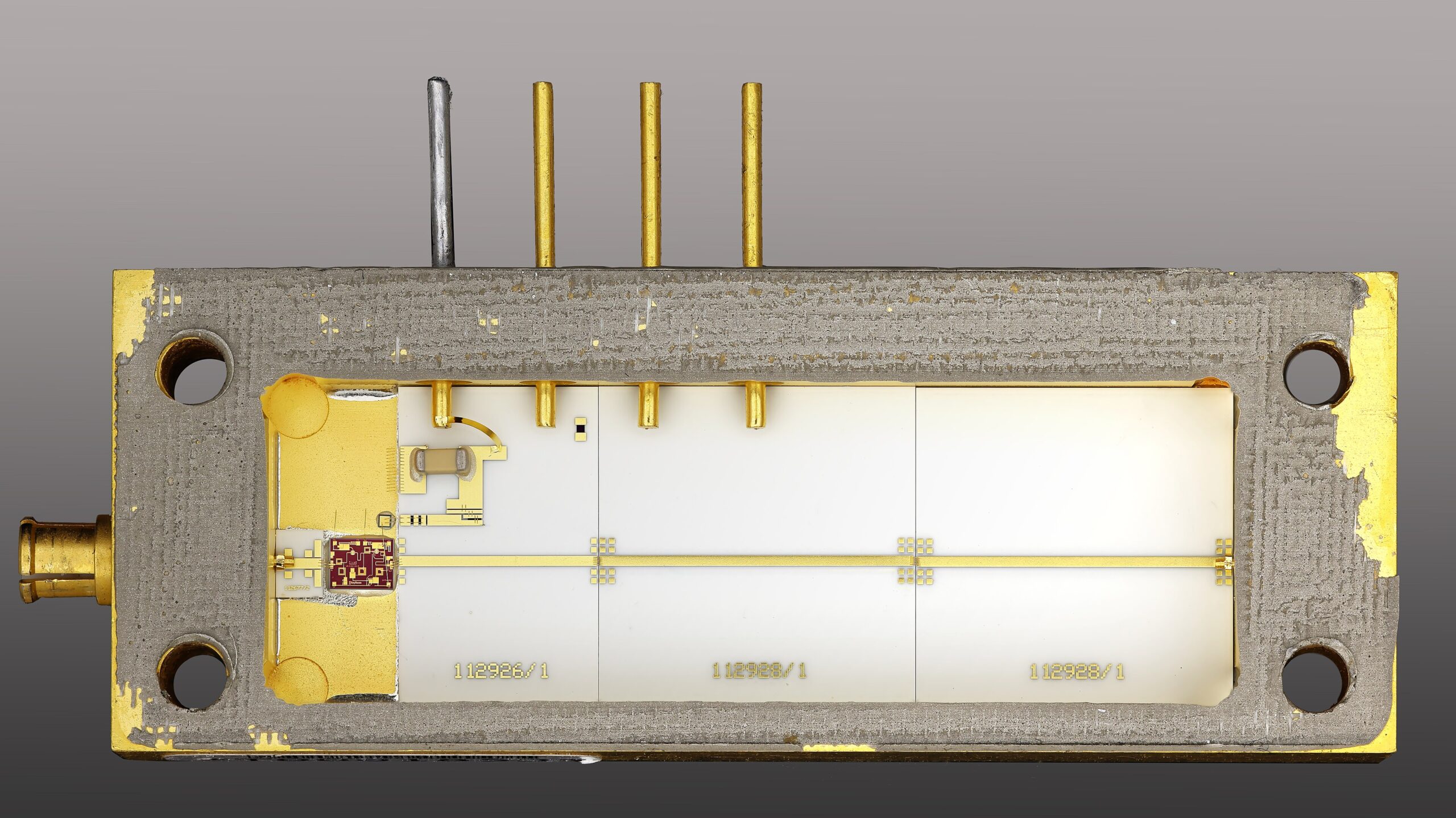
This opened low-noise amplifier (LNA) module, an amplifier built to add little noise, shows the route: die, wire bonds, metal housing.
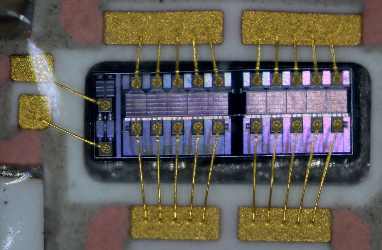
Closer in, an old handset hybrid power amplifier (PA, the stage delivering the output signal) shows die attach and bonds.
QFN and small plastic packages: not automatically off-limits
The Mini-Circuits 2021 article shows optimized over-molded QFN examples (plastic molded around the die) reaching 50 GHz (gigahertz, billions of cycles per second). These are one vendor’s optimized examples, not a rating for every QFN or a power rating.
The better question is whether the RF transition between board and package is designed and measured at your frequency. The WAVEPIA packaging page names ceramic MMIC packages (MPKG2, MPKG3.1) beside leadless carriers, QFN and transistor packages, in its own words.
Ceramic cavities, flanges and sealed housings solve different problems
Three problems hide here: an air space above the circuit for RF, heat removal, and environmental protection. An air-cavity package leaves that space and can be plastic or ceramic.
A flange is a metal base that bolts or clamps to a heat sink. In one example path, heat travels from the die through the die attach, any carrier or heat spreader (a plate that spreads heat sideways; not always present), the flange, the flange-to-heat-sink interface (thermal interface material, solder or clamping) and into the heat sink. Mounting and interface conditions often dominate. This path is our engineering reasoning, not a cited rating; the part’s mounting drawing and thermal data govern.
Hermetic does not mean an absolutely perfect, gas-tight seal. It means limited gas and moisture exchange, demonstrated against a specified leak-test criterion. A lid, air cavity or ceramic body does not show that by itself, so ask for the method, the limits and which assemblies were tested. For ceramic and aluminum nitride materials, see our earlier ceramic-package post.
GaN amplifiers: review bias order and heat path together
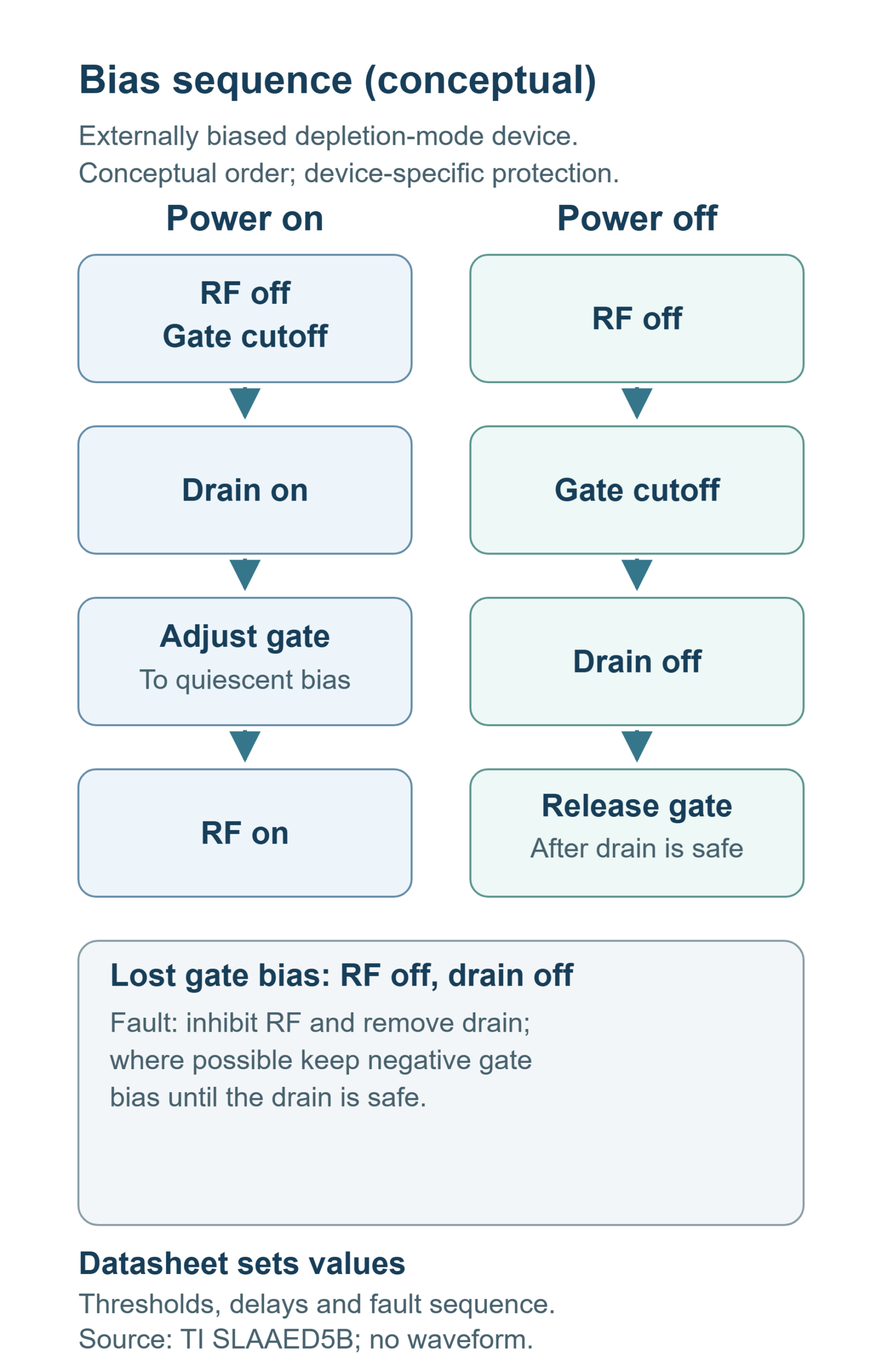
In an externally biased depletion-mode GaN device, the drain (main supply terminal) carries current through the channel (the conducting path inside the transistor) until the gate is at or more negative than the device’s pinch-off (cutoff) voltage, the term in TI’s note, within the datasheet’s gate-voltage limits. A gate that is negative but less negative than cutoff may still conduct. The cutoff value is device-specific and none is given here. Texas Instruments’ note SLAAED5B (revised May 2026), page 4 section 3, gives the normal order:
- Power up: set the gate to cutoff, apply the drain, adjust the gate to the device-specified quiescent bias (the operating point with no input signal, which the datasheet may state as a current target), then apply RF.
- Shut down: remove RF, return the gate to cutoff, remove the drain, then release the gate once the drain is safely removed.
A fault is a separate case from this orderly shutdown. If negative gate bias is lost, the gate may never reach cutoff, so protection should not wait for cutoff while the channel conducts; it should inhibit RF and disable the drain. An interlock, meaning protective logic that disables the RF and the drain when conditions are unsafe, does this job. Where possible, keep negative gate bias until the drain is safely removed or discharged. TI’s note covers monitoring for lost negative bias (page 10 section 11); its page 8 section 8 shows one example controller whose alarm forces its power-amplifier enable signal low to disable the drain path. That is an example implementation, not a universal response or a promise that cutoff can be restored during a failure. The datasheet and the interlock design govern the fault response; no voltages, currents or response times are given here. Bias also interacts with temperature (page 3), so review it with the thermal path above.
Sourcing in China: who does what, and the evidence to request
The engineering above applies anywhere. Public vendor pages show what some China-based suppliers say they offer, and their roles differ. These are attributed statements, not recommendations.
- JCET advertises system-in-package (SiP, several chips and parts in one package) integration. Its page names RF front-end (the circuits between the antenna and the receiver or transmitter) and power-amplifier modules, with SMT, wire bond, flip chip (face-down bumped chip), shielding and dual-sided integration.
- AlN China (上海芯陶微新材料有限公司) (AlN means aluminum nitride, a ceramic) lists package bodies and lids: high-temperature co-fired ceramic (HTCC, ceramic layers fired with metal), ceramic QFN and plastic air-cavity packages. It also advertises a ceramic QFN microwave-chip packaging solution (cards dated 05/2026).
- Hebei Sinopack lists ceramic and thermal components: wireless-communication ceramic housings, aluminum nitride substrates and tungsten-copper heat-spreading components.
These pages do not establish test band, qualification (a formal test program showing a part meets stated requirements), capacity, price, lead time or access. Confirm the exact assembly and test scope and the performing facility with the supplier for your project; no qualified capacity or access is claimed here. The checklist applies to any supplier, anywhere.
| Ask for | Why it matters |
|---|---|
| RF data and test fixture | Measured gain, loss and return loss (a measure of how much RF signal reflects back) at your reference plane and band, with the test fixture (the jig and adaptors that connect the part for measurement) described |
| Thermal data and mounting | Attach, thermal interface, heat sink and mounting conditions; a rating without them does not transfer |
| Die attach | Method and materials matched to your thermal path |
| Wire bonds | Layout and inspection records |
| Seal and leak test | Method, limits and assemblies tested |
| Qualification scope | Which die, package and assembly combination |
| Performing facility | Where each step is done |
| Change control | Notice of material or process changes |
Selected primary sources
- Mini-Circuits, 26 Feb 2021: optimized QFN examples to 50 GHz; manually intensive bare-die assembly and limited die-on-carrier protection.
- WAVEPIA, undated: named ceramic MMIC and carrier packages.
- Texas Instruments SLAAED5B, rev. May 2026: bias sequence, negative-bias monitoring, example alarm-driven drain disable, bias and temperature.
- JCET system-in-package, undated: SiP module and assembly statements.
- AlN China (上海芯陶微新材料有限公司), solution cards 05/2026: HTCC, ceramic QFN, lids, ceramic QFN packaging solution.
- Hebei Sinopack, undated: ceramic housings, substrates, thermal components.
Next step: write one paragraph with the function, band, reference plane, heat sink and environment, then request these items for that exact die, package and assembly combination.
Related reading: our post on ceramic packages for high-voltage integrated circuits.
Please link to this article when sharing. Contact us for permission to republish the full article.