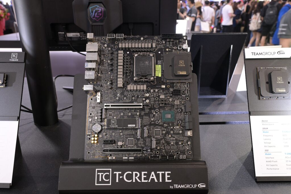
A CPU or GPU VRM is the complete local power supply that turns a higher board voltage into the low, tightly regulated rail a processor uses. DrMOS is one part of it, not the whole regulator.
This article covers the common multiphase buck architecture used for many CPU and GPU core rails, not every accelerator design.
Three takeaways
- A VRM is a system: controller, power stages, inductors and capacitors working together.
- Phase count multiplied by a power-stage rating is not usable board capacity.
- TLVR (trans-inductor voltage regulator) is a multiphase buck design that adds a magnetic coupling loop for faster current response. It does not replace DrMOS or isolate the processor.
What a CPU or GPU VRM does
A processor wants a low voltage and a very large current that can change in nanoseconds. TI’s TLVR seminar describes high-end core rails that in some cases have thermal design currents above 1,000 A, peak currents above 2,000 A and nanosecond-range rise times, at about 0.7 V ±3%.[1]
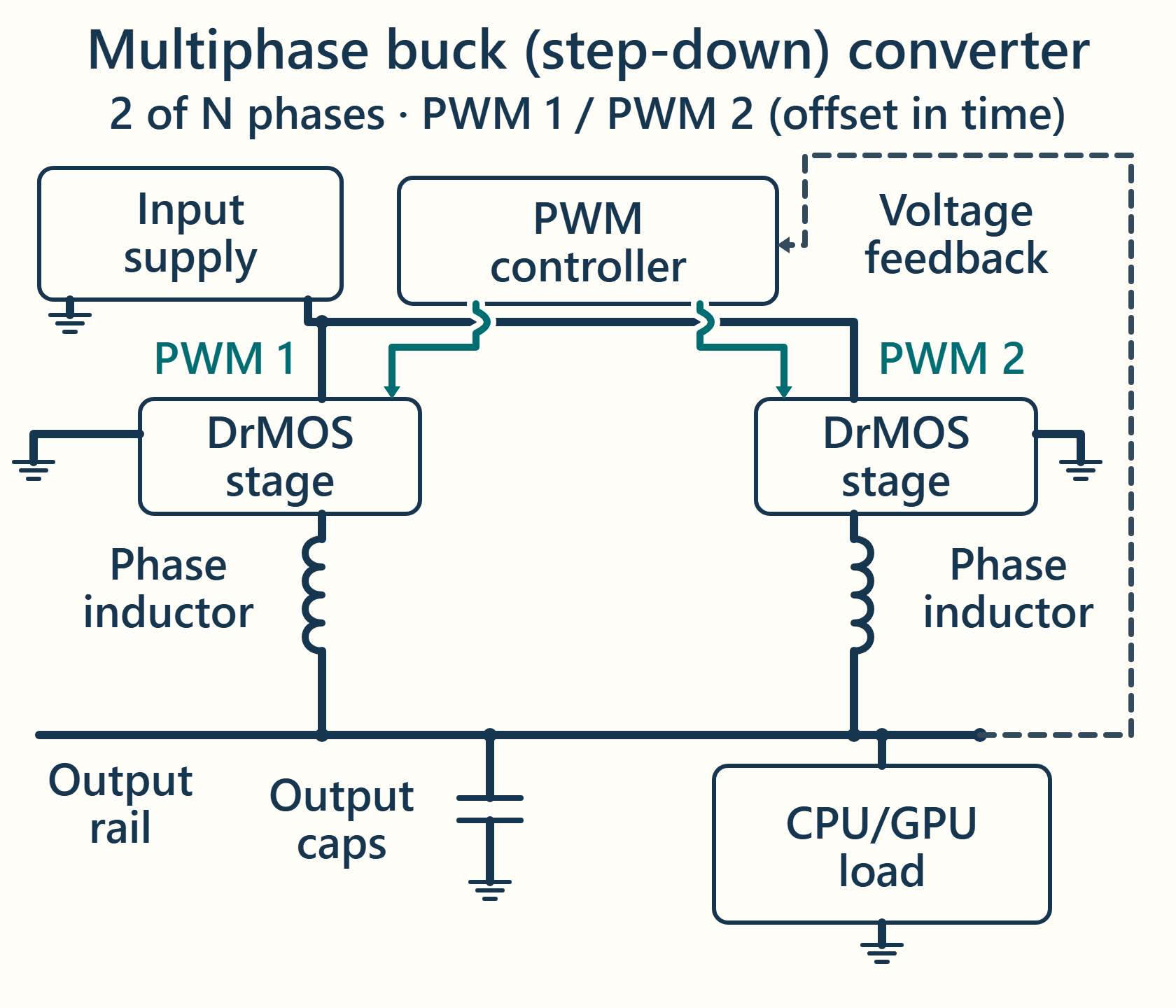
The usual answer is a controlled multiphase buck converter. A controller sets switching timing and watches the output, power stages chop the input, and inductors and capacitors smooth the result into the final rail.[1][3]
Where DrMOS fits
DrMOS is the power stage: one package holding a driver IC (the chip that commands the switches) and switching MOSFETs (the power transistors that chop the input). TI describes its CSD95410, for example, as integrating the driver IC and power MOSFETs, plus current and temperature sensing.[4] The controller, phase inductors and output capacitors remain separate parts of the regulator.
TI’s public TPS53689T overview shows what a controller looks like: a multiphase part with TLVR support and an Intel VR14 SVID interface (a CPU-side control link to the regulator).[3] That is a CPU-side interface; this one example does not establish a general GPU interface. Sensing and protection features also vary by stage, so a name or photo does not reveal them.
What phases do
A phase is one switching stage plus its inductor. The controller staggers the phases, so input and output ripple currents offset each other and heat spreads across more devices.[5]
The hard part is current sharing. Sensing offsets, component tolerances and temperature differences cause imbalance, and during a load transient it can saturate an inductor and cause overheating.[5] Three distinctions help:
- Rails versus phases. A rail is a separately regulated output. Phases are parallel contributors to one rail.
- Independent PWM versus counted parts. Inductors or packages on a board do not prove how many independently timed PWM channels exist.
- Doubled versus teamed stages. “Teamed” is board and vendor terminology, not a universal standard term. Renesas’s public ISL6617 datasheet, from 2010 for a product now listed as obsolete, shows a doubler taking one PWM input and driving two PWM outputs, with interleaving and synchronous modes.[6] So a doubled pair is not necessarily in lockstep. ASUS describes its teamed power-stage architecture as two power stages working in tandem; that page is undated, comes from the X570 era, and is cited here for that one statement only.[7] As a general engineering description, not a statement from either source, stages driven by one shared PWM signal act as one larger phase, while stages driven by phase-shifted outputs can still interleave. Implementations differ, and no design should be assumed identical to another.
Why voltage changes when load changes
Inductor current cannot jump. When load current steps up, the summed inductor current ramps toward it, and the output capacitors supply the difference meanwhile. That charge deficit makes the voltage undershoot; a load release causes overshoot.[1] Designers limit it with faster current ramping, meaning lower inductance, or with more output capacitance. Lower inductance raises ripple and root-mean-square (RMS) current and costs efficiency.[1]
A load-line is different. Adaptive voltage positioning intentionally lets output voltage fall as load current rises, starting near the top of the allowed window. It can reduce the capacitance needed and applies to conventional and TLVR designs alike.[1] A lower voltage under steady heavy load may therefore be designed behavior; undershoot during the step itself is the transient.
What TLVR changes
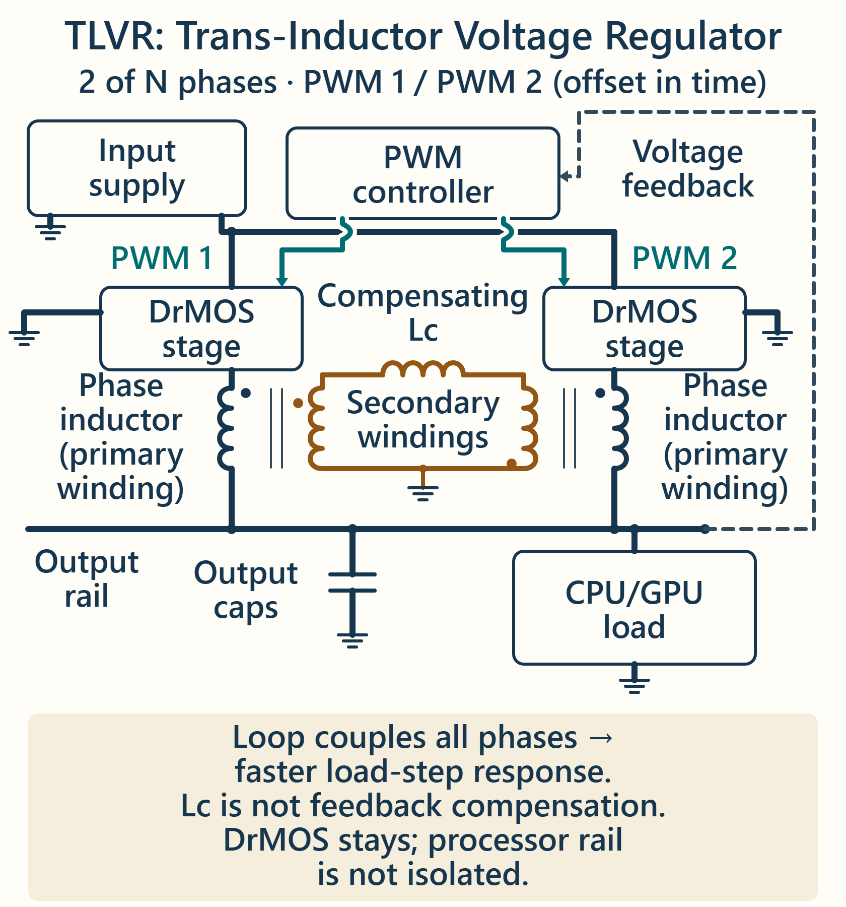
TLVR keeps the multiphase buck but replaces each phase’s single-winding inductor with a two-winding coupled inductor. The primary winding still runs from the switch node to the output. The secondary windings join in one series loop with a compensating inductor, Lc.[1][2]
TI’s stated aim is a high effective inductance in steady state, limiting ripple and RMS loss, and a low effective inductance during transients so current ramps faster.[1]
Three clarifications:
- Lc belongs to a magnetic loop. It is not feedback compensation; voltage feedback still returns to the controller.
- DrMOS stages remain, and primary current still reaches the processor rail, so the rail is not galvanically isolated.
- Benefits depend on implementation. Infineon warns that if Lc saturates and current ramps steeply, the coupled inductors can saturate too and the controller can lose control.[2] Capacitance savings are design-specific, not guaranteed.
How to read a VRM specification
Treat each line of a specification as a question about the whole regulator.
| Specification line | What it tells you | What to check next |
|---|---|---|
| Phase count | Parallel contributors to a rail | Independent PWM channels, doubled or teamed stages, current sharing |
| Power-stage current rating | A component rating under stated conditions | Cooling, switching frequency, inductors, board layout and protection limits |
| “Smart” stage features | Sensing or protection options that vary by part | Which signals actually reach the controller |
| Load-line setting | Intentional voltage slope with load | Allowed voltage window and measured transient response |
| TLVR | Coupled inductors with a secondary loop and Lc | Lc value, saturation margin and the capacitance actually used |
Treating a rating as board capacity is unsafe. That is an engineering inference, not a vendor statement: cooling, switching conditions, current sharing, magnetics and protection all limit what a board delivers.[4][5]
A quick checklist:
- Which parts are named, and which are only implied?
- Are phases independent, doubled or teamed?
- Is a voltage drop a load-line or a transient?
- Does TLVR come with stated magnetics and capacitance conditions?
A VRM specification is a map of questions, not a score. Once you can place each part and see which problem it solves, phase counts, DrMOS and TLVR claims become easier to judge.
Sources
- TI, Introduction to the Trans-Inductor Voltage Regulator (SLUP413A, April 2026): core-rail demands, winding arrangement, charge deficit and load-line.
- Infineon, Multiphase buck converter with TLVR output filter (application note V1.4, May 2025): series secondary loop, Lc and saturation.
- TI, TPS53689T product page: an example controller with TLVR support and VR14 SVID.
- TI, CSD95410RRB product page: a power stage integrating driver and MOSFETs.
- TI, Phase current sharing technical article (SSZTC61, September 2015): interleaving and current balance.
- Renesas (formerly Intersil), ISL6617 PWM doubler datasheet (FN7564 Rev 0.00, 4 February 2010): one PWM input, two PWM outputs, interleaving and synchronous modes. A legacy part, now listed as obsolete; cited for the physical principle only, not as a recommendation.
- ASUS, Teamed Power Architecture (undated vendor page, X570-era legacy context): two power stages working in tandem. Used for the terminology only; no heat or performance claim is taken from it.
Related reading
Featured image: motherboard exhibit by 4300streetcar, 23 May 2025, CC BY 4.0, via Wikimedia Commons. The recommended file is the unedited 3,840 px Commons rendition; the site theme may crop it for display. It is generic context and does not identify any specific VRM design.
Please link to this article when sharing. Contact us for permission to republish the full article.