
When a removable AI-server board or compute tray meets an energized 48/54 V backplane, its input protection circuit faces several different jobs in rapid succession. It must charge the board capacitance without collapsing the source or damaging the pass switch. It must then carry high steady current with manageable loss. It must tolerate legitimate workload steps without nuisance trips—and disconnect a hard short quickly enough to prevent destructive energy from accumulating.
Those jobs explain why the useful design question is not simply, “Which device has the largest current number?” It is: under the same voltage, transient, safe-operating-area, thermal and fault-response envelope, when does an integrated smart eFuse make more sense than a hot-swap controller driving external MOSFETs?
This is a board-level decision inside the wider transition from 48 V racks toward higher-voltage AI infrastructure. It remains relevant even as the industry develops 800 VDC distribution for future AI factories.
Key Insights
- A nominal 48/51/54 V application does not make every “80 V-class” product equivalent. Recommended operation, absolute maximum, internal-switch rating and time-limited surge withstand are different specifications.
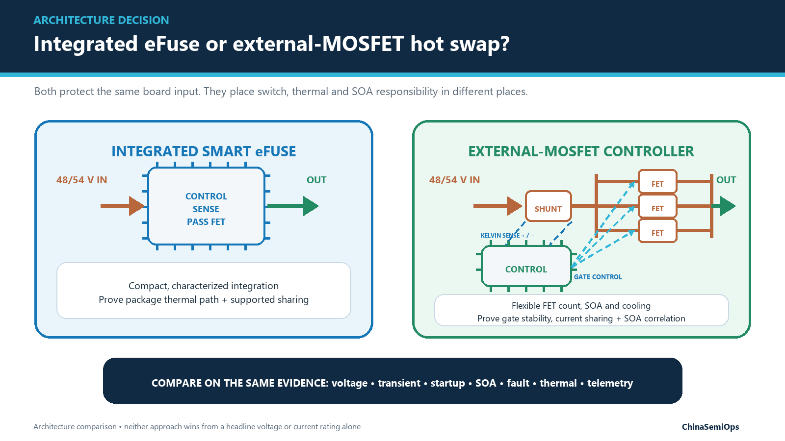
- An integrated eFuse combines more of the control, sensing and pass switch in one characterized device. An external-FET controller gives the designer more freedom to scale resistance, current, cooling and linear-mode SOA.
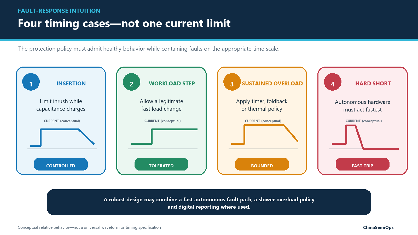
- Insertion, workload steps, sustained overload and hard short are four different timing cases. One current-limit number cannot describe them.
- PMBus telemetry and fault history improve observability. The fastest protection against a severe short still needs an autonomous hardware path.
- The category is contested, not empty. Current TI, Infineon and Analog Devices products illustrate different integration and scalability choices.
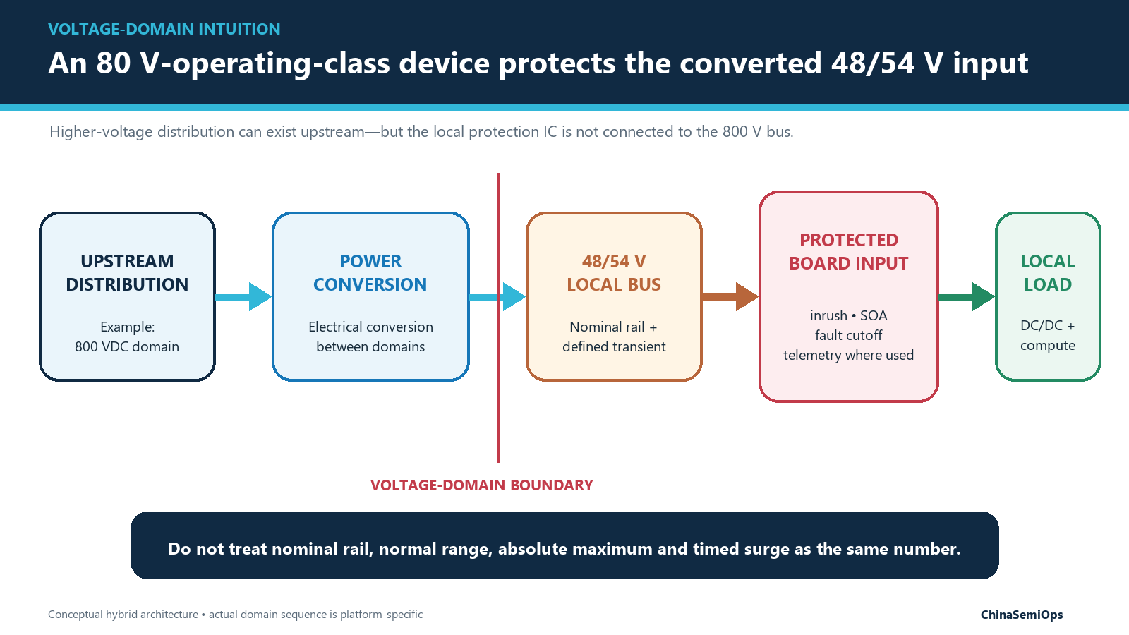
Why a Nominal 48/54 V Bus Uses 80 V-Class Protection
The Open Compute Project’s Open Rack Wide specification expects a nominal 51 VDC input from an Open Rack V3 power shelf and normal IT-gear operation across 46 V to 52 V. Other platforms and vendor material commonly use “48 V” or “54 V” for related—but not necessarily identical—domains. Engineers therefore need the actual system envelope, not only the customary rail name.
A product comparison should keep at least five voltage definitions separate:
- the nominal system rail;
- the required normal operating window;
- the defined transient waveform and source impedance;
- the IC’s recommended operating range; and
- the IC’s absolute-maximum and any separately specified timed-surge limits.
For example, TI specifies 9 V to 80 V recommended operation for TPS1689 and a 92 V absolute maximum at the stated condition. That does not make 92 V a normal operating point. Likewise, a vendor’s description of an internal 100 V MOSFET or a short-duration surge capability is not the same as a 100 V continuous input rating.
The required margin depends on the real bus, connector, harness, hot-plug inductance, suppression network, upstream source and fault cases. “80 V-class” is therefore a useful architectural label, not a substitute for a transient specification.
Higher-voltage distribution can exist upstream while an electrically separate, converted 48/54 V domain still needs local board protection. An 80 V-class eFuse does not connect to or protect an 800 V bus; that is a separate protection problem at an emerging 800 V rack boundary.
What Makes an eFuse “Smart”?
A conventional fuse responds to excess current by permanently opening. A smart eFuse or hot-swap circuit can implement a richer, resettable power-entry policy:
- controlled output ramp and inrush limiting;
- undervoltage and overvoltage response;
- current sensing and programmable current limiting;
- a fast trip path for severe overcurrent;
- a slower timer or foldback policy for sustained overload;
- switch-temperature and safe-operating-area protection;
- latch-off, retry or host-controlled recovery;
- current, voltage, power and temperature monitoring; and
- fault status, configuration and event history.
Not every design needs every digital feature, and more telemetry does not make a protection loop inherently faster. PMBus can help configure limits, observe margin and explain a fault after it happens. It should not be the only mechanism expected to stop a rapidly developing short. The severe-fault path must remain deterministic even when the host processor is unavailable or the management bus is busy.
“Smart” is most useful when it describes coordinated behavior—not simply the presence of a digital interface.
Integrated eFuse or External-MOSFET Controller?
Both architectures control the same fundamental boundary: an energized source, a capacitive downstream load and a pass element that must survive startup and faults. Their division of responsibility is different.
| Decision dimension | Integrated smart eFuse | External-MOSFET hot-swap controller |
|---|---|---|
| Power path | Control, sensing and pass switch are substantially integrated | The controller manages a selected external MOSFET bank and current-sense element |
| Primary advantage | Compact implementation with characterized internal relationships | Flexible MOSFET count, resistance, cooling and linear-mode SOA |
| Current scaling | Parallel or stack only as the product permits; sharing must be validated | Scale through MOSFETs, sense elements and, in some designs, parallel controllers |
| Thermal boundary | The package and PCB remove heat from the integrated switch | Heat can be distributed across selected external switches and board area |
| SOA responsibility | Vendor protection model plus system-level validation | Designer must correlate the actual MOSFET SOA with gate control, timing and temperature |
| Telemetry | Product-specific analog monitoring and/or PMBus | Product-specific PMBus/SMBus monitoring, often with external-switch measurements |
| Integration cost | Less freedom to change the pass element | More BOM, layout, parasitic and validation responsibility |
| Typical reason to choose | Density, repeatability and compact integration dominate | Power level or fault envelope demands switch flexibility |
TI’s TPS1689 illustrates the integrated approach. TI lists the device as ACTIVE and specifies 9 V to 80 V recommended operation, a stackable 20 A eFuse with an adjustable 2 A to 20 A overcurrent threshold, and PMBus telemetry. The Rev. A datasheet revised in December 2025 is labeled PRODUCTION DATA and gives 3.5 mΩ typical on-resistance at its stated test condition. Those numbers describe one device; a parallel or stacked system needs its own sharing, PCB and thermal validation.
Infineon’s XDP730/XDP72x family represents another integrated direction. The company describes 7 V to 80 V devices with 20 A or 30 A-class integrated pass paths, active SOA control and PMBus on selected variants. As observed on July 28, 2026, Infineon had announced the family and stated sample/evaluation availability, while live part pages still displayed “coming soon.” That is evidence of active product development, not proof of volume production or deployment.
Analog Devices’ LTC4286/LTC4287 family illustrates the external-MOSFET controller approach. Analog Devices currently lists LTC4287 as recommended for new designs. It supports a 6.5 V to 80 V input range, drives two gates, uses multimode startup control to manage MOSFET SOA, and provides power monitoring with an SMBus interface and PMBus-compliant command structure.
At much higher board current, the reason for retaining external switches becomes visible. TI’s PMP23496 is a tested 54 V, 150 A RMS, 8.1 kW reference design using an LM5066I controller and nine external MOSFETs. It is not an 8.1 kW IC rating, a shipping server or evidence of fleet deployment. It is a public engineering example of how an external-FET bank can scale a protected power path.
Four Timing Cases—Not One Current Limit
1. Insertion
At connection, uncharged downstream capacitance initially demands current. The protection circuit controls the voltage ramp so the connector, source, pass device and PCB remain inside their intended stress envelopes. During this interval, the pass switch can dissipate substantial power in linear mode, so its SOA and transient thermal impedance may matter more than steady-state on-resistance.
2. Workload Step
Accelerators and downstream converters can produce legitimate, fast load changes. The protection design must distinguish those events from faults. Otherwise, a threshold chosen only for fast short-circuit protection can create nuisance trips during normal computation.
3. Sustained Overload
A load above the normal envelope but below the severe-short threshold needs a bounded current-versus-time policy. Depending on the system, that may involve a circuit-breaker timer, foldback, thermal supervision, retry or latch-off. There is no universal best recovery policy.
4. Hard Short
A severe short requires an autonomous response before the pass device, connector or copper path absorbs destructive energy. Detection delay, gate discharge, parasitic inductance and clamp behavior all affect the result. Digital reporting can record the event, but it is not the first line of protection. This is the board-level version of why protection timing becomes harder as voltage and fault energy rise.
A robust design may therefore combine a fast analog severe-fault path, a slower overload policy and a digital observation layer. The correct thresholds and timing must come from the tested board, pass device, capacitance, inductance and temperature—not from a universal “AI workload” number.
A Design-Review Evidence Checklist
When comparing devices or architectures, ask for the same evidence on both sides:
- What are the nominal, minimum and maximum bus voltages?
- What transient waveform, duration and source impedance must be survived?
- What input capacitance must be charged, and how quickly?
- What are the steady and peak currents at the actual package and board temperatures?
- Does the pass-device SOA cover the required voltage, current, pulse width and temperature during startup and faults?
- How are severe-short and sustained-overload responses defined and tested?
- For parallel devices, how are current sharing and thermal imbalance managed?
- For an external bank, how is MOSFET balance and gate behavior controlled?
- What PCB area, airflow, cold plate or other cooling boundary is assumed?
- What are the telemetry accuracy, bandwidth and calibration conditions?
- What happens after a trip: retry, latch, brownout recovery or host command?
- Is the evidence for a released product, a preliminary sample, an evaluation board, a reference design or a production deployment?
Evidence rule: A product page, an evaluation board and a shipping customer deployment are different evidence levels.
The available products do not establish one universal winner. They show a contested category in which integrated eFuses prioritize compact, characterized integration while external-FET controllers retain more freedom to scale the power switch and its thermal environment.
Protection Is Behavior, Not a Headline Rating
The first component at a removable board input must admit healthy power, reject unsafe power and leave enough evidence to diagnose what happened. Selecting it from a voltage or current headline alone ignores the hardest part of the job.
The strongest 48/54 V protection design is the one whose startup, SOA, fault, thermal and telemetry behavior is proven together on the intended board. Integrated eFuses and external-MOSFET controllers can both be credible—but only when they are evaluated against the same operating and fault envelope.
Evaluating a 48/54 V AI-server power path? Start with that envelope, not a headline rating. Define the bus transient, input capacitance, startup time, switch temperature, hard-short response and telemetry requirement, then compare the two architectures on equal terms. ChinaSemiOps welcomes public-source, non-confidential discussions about framing that comparison.
A 48/54 V high-current bus can present serious arc, thermal, connector and fire energy. “Hot-swappable” does not mean exposed energized hardware is inherently safe to service. The IC is one layer in a coordinated system that also depends on connector sequencing, PCB and bus impedance, upstream protection, discharge, thermal design, enclosure and service procedure.
This article is an engineering framework, not a component recommendation, safety design, market forecast or production specification.
Selected Public Sources
- Open Compute Project — Open Rack Wide Base Specification V1.0
- Texas Instruments — TPS1689 product page
- Texas Instruments — TPS1689 Rev. A datasheet
- Texas Instruments — PMP23496 8 kW hot-swap reference design
- Infineon — XDP730-001 product page
- Infineon — XDP730 datasheet
- Analog Devices — LTC4287 product page and datasheet
Related reading: smart power-path functions beyond the data center.