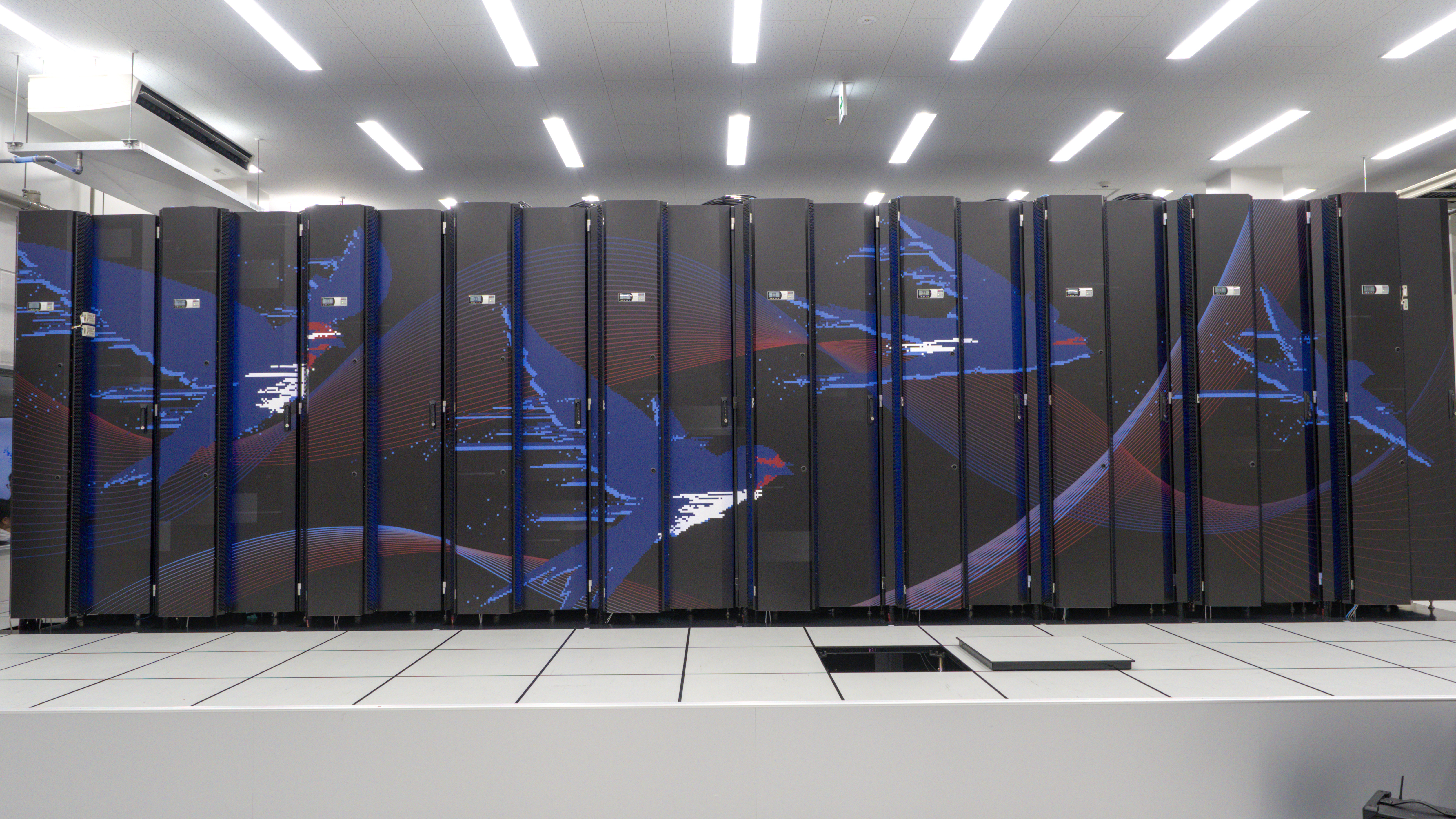
Application context; the package memory and proposed architecture are not shown.
Where memory sits next to a processor chip changes how much data it can hold, how quickly data moves and how heat leaves the package around the chips. This article follows that heat path and ends with a six-row worksheet for comparing stacked-memory proposals on matching assumptions.
When an AI (artificial intelligence) accelerator needs more memory, the design must decide where the next memory die (a single memory chip) goes: beside the processor, on top of it, or standing on edge above it. Each answer changes how much data fits, how quickly it moves and, less obviously, how heat leaves the package.
The memory involved is DRAM (dynamic random-access memory), the main working memory that holds data during computation. HBM (high-bandwidth memory) is a stack of DRAM dies joined by many parallel connections. The processor it sits beside or beneath is the GPU (graphics processing unit), the chip that performs most of the arithmetic in AI training.
Start with what actually limits the workload
Capacity is how much data memory can hold; bandwidth is how much it can deliver per second. A model that does not fit in memory needs capacity. A model that fits but keeps waiting for data needs bandwidth. When the arithmetic itself sets the pace, the workload is compute-bound, and more memory of either kind helps little. “Add more memory” therefore hides at least three questions, and a proposal that answers only one has not yet shown that anything gets faster.
Three ways to place memory around a GPU
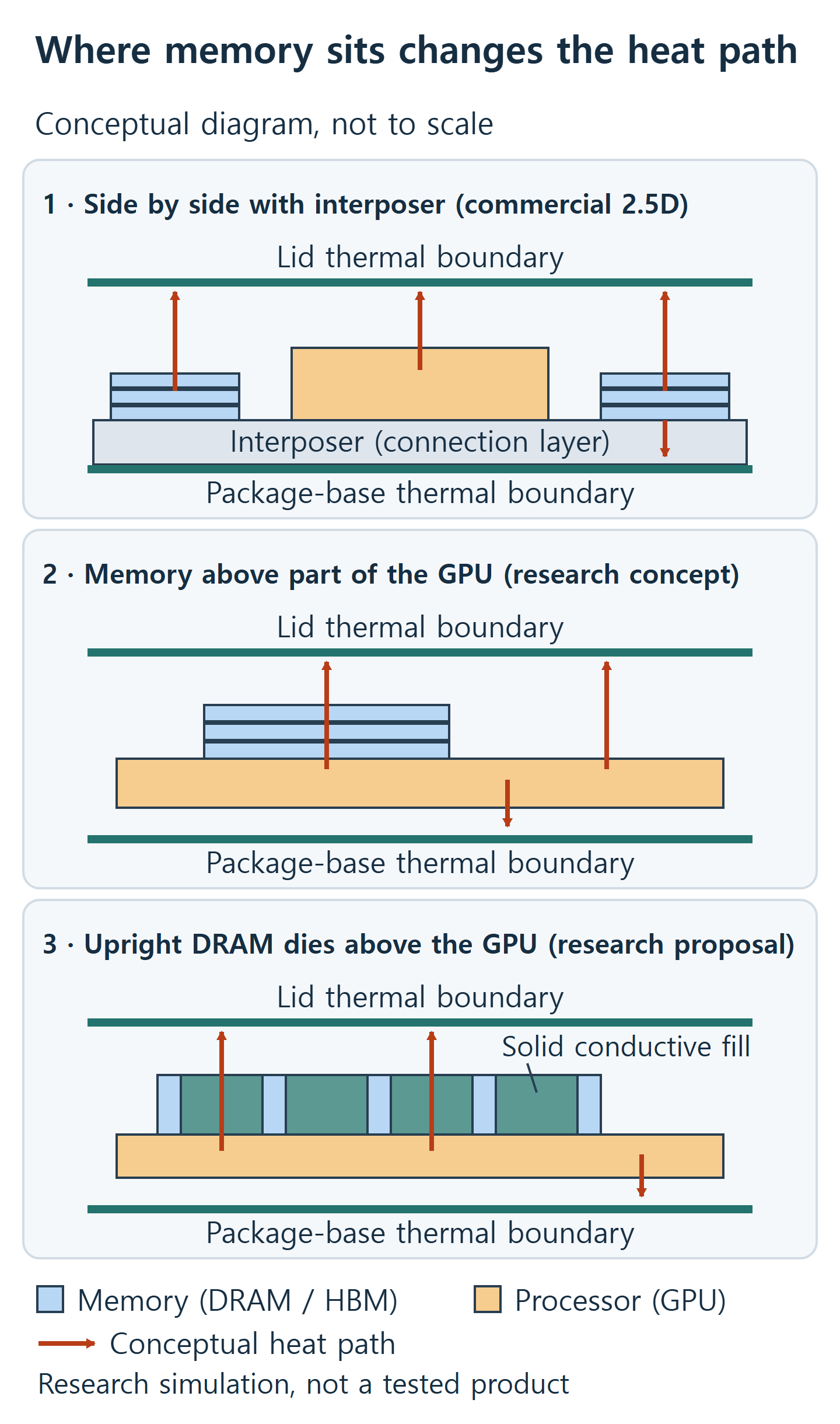
Today’s commercial approach is 2.5D packaging: the GPU and HBM stacks sit side by side on an interposer, a thin layer that carries the many signals between dies. TSMC describes its CoWoS (Chip-on-Wafer-on-Substrate) platform this way, in the CoWoS-S version that uses a silicon interposer, and reports production milestones beginning in 2012. Those are the vendor’s own statements; they do not cover who can obtain it.
3D packaging stacks dies on top of one another. In a December 2025 press release, imec describes a simulation study of HBM placed directly on a GPU, evaluating thermal and system mitigations such as double-sided cooling and frequency scaling (adjusting clock speed).
A September 2026 preprint, a paper posted openly on arXiv (version 1; see also its arXiv record), simulates a third option: DRAM dies standing upright above the GPU, rotated relative to ordinary flat stacking. Between the upright dies the paper places “cooling cavities.” Despite the name, these are regions filled with solid conductive material (silicon, copper or diamond in the studied designs), not channels for flowing fluid.
For a flat comparison point, the paper modifies an earlier HBM-on-GPU design so that customized DRAM covers the GPU in place of thermal silicon. That reference is the paper’s own modification, not a commercial product and not the unchanged design described in imec’s December 2025 study, and imec’s study does not independently replicate the paper.
Every comparison also needs thermal boundary conditions: stated assumptions about how heat leaves the modeled package. Here there are two, the lid (the cover on top of the package) and the package base (the laminate, the layered substrate underneath). The paper matched both across the designs it compared.
The diagram sketches the three arrangements. Panel 1 draws an interposer because of the commercial 2.5D context above; panels 2 and 3 are research concepts.
Trace the heat path before reading any result
Heat does not start evenly. A spatial power map shows how power, and therefore heat, is distributed across the die area. A hotspot is the small region where temperature peaks. Moving memory changes what stands between those regions and the lid or package base: bonded interfaces, mold (the compound that fills space around the dies), silicon or solid fill.
The paper simulated its designs with one nonuniform GPU power map. In those models, taller stacks raised the peak temperature, and the fill material and memory arrangement changed the resulting range. Mold interrupted sideways heat spreading. Rotating the dies redistributed temperatures: much of a die could improve while its peak got worse.
A lower average temperature is not a lower hotspot, and these results belong to specific modeled layouts, not to general thermal limits.
Compare useful work under stated conditions
The paper also simulated training of one specific language model, Qwen3-32B, on several configurations. In its model, stack height can add capacity without adding interfaces, while more active dies add bandwidth. For that workload, training gains flattened once execution became compute-bound; other workloads may behave differently. The flattening is a workload effect, not thermal throttling (hardware slowing itself to limit temperature). Capacity also changes how work is split across processors and how much they must communicate, so extra memory does not translate directly into speed.
Judge a memory option on useful work under stated heat conditions, and on how mature its evidence is: simulated, measured or qualified. Qualification means testing that shows a part meets the reliability requirements for production use. Both studies above are simulations; neither shows qualification or availability.
A six-row worksheet for the next design review
This worksheet is our suggested review method, not a standard drawn from the sources. It applies generally to accelerator designers, memory suppliers, packaging providers, thermal engineers and test or assembly owners, wherever the work is done.
| # | Ask | Why it matters |
|---|---|---|
| 1 | Do all options use the same model, software, batch size (how many examples are processed together) and numeric precision (how many bits represent each number)? | Otherwise performance numbers are not comparable. |
| 2 | Are capacity and bandwidth stated separately, with the limit that actually binds? | Storing data and moving data fail differently. |
| 3 | Are the spatial power map and the lid and package-base boundaries identical? | Temperatures compare only under matching assumptions. |
| 4 | Which interfaces, mold regions and hotspots lie between the GPU and each boundary? | Geometry decides where peaks form. |
| 5 | Is the evidence measured or simulated, and what remains before qualification? | Feasibility is not readiness. |
| 6 | Who owns assembly, inspection, test and each missing piece of evidence? | Gaps without an owner stall. |
What to settle first
Rows 1 to 3 are assumptions to align, and feasibility work can help settle them. Declare the workload, the binding limit and the thermal boundaries before comparing performance, then use rows 4 to 6 to scope the remaining engineering work.
Sources
- arXiv preprint 2609.24343, version 1 and submission record: submitted September 21, 2026.
- imec press release: December 8, 2025.
- TSMC CoWoS platform page: undated vendor page, checked October 28, 2026.
Please link to this article when sharing. Contact us for permission to republish the full article.