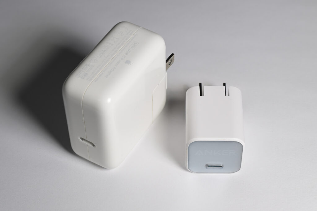
Two power-adapter enclosures provide application context. Internal devices are not shown. Photo: 4300streetcar / Wikimedia Commons, 25 December 2025, Creative Commons Attribution 4.0.
Suppose you are choosing the switching stage for a compact adapter. The product page says "integrated driver and protection," and the schedule is tight. Before you mark the gate driver—the circuit that turns a power switch on and off—as covered, you need answers to a few plain questions. Which bias supply, the power that runs the driver itself, is needed? Who powers the upper switch? Who carries the command signal to it? Who reacts when current runs away?
GaN (gallium nitride, the semiconductor material used for the fast power switch) power ICs (integrated circuits, semiconductor circuits combining multiple electronic functions) answer those questions differently from part to part. For GaN power ICs, a worksheet filled in before selection is cheaper than finding the gaps on the bench.
Key takeaways
- "Integrated" can mean a driver alone, a switch with its driver, or a switch with driver and protection. Compare the functions actually listed for your exact part.
- One package is not the same as one chip, and a datasheet or product page may not say which you have.
- Before selection, mark every function as included, external, or an open question for the supplier.
Start with the functions your converter needs
Take a half-bridge: two switches stacked between the supply and ground, with the "high-side" switch toward the supply and the "low-side" switch toward ground. A controller decides when each one conducts. Each switch is a FET (field-effect transistor, an electrically controlled switch), and a gate driver is the circuit that switches it on and off by charging and discharging its gate, the control terminal.
The functions worth listing are:
- Gate drive for each switch.
- Bias: the power supply that the driver and control circuits themselves need.
- A supply for the high-side driver, whose reference voltage moves with the switch.
- Dead time: a short interval with both switches off, to prevent both conducting together and connecting the supply to ground (shoot-through).
- A signal path from the controller to the high-side switch.
- Overcurrent protection (OCP) and short-circuit protection (SCP): the device's response to excess current.
- A system-level fault response: what the converter does after a fault.
- A path for heat to leave.
Read two documented integration boundaries
Two Texas Instruments (TI) datasheets show how different the boundary can be. They are different voltage classes and building blocks, so read them side by side, not as a ranking.
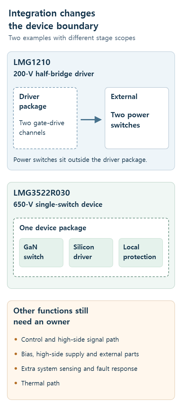
The LMG1210 datasheet (revision January 2019) describes a 200-V half-bridge driver with two gate-drive channels for external switches. An internal regulator holds the gate-drive voltage at 5 V, yet the design still includes external bypass capacitors, which help keep the local supply steady, and a bootstrap capacitor, with an external bootstrap diode the designer chooses. Bootstrap means a diode-and-capacitor arrangement that charges the high-side supply while the switching node—the midpoint between the two switches—is at low voltage. In its independent-input mode the dead-time circuit is inactive and the controller must prevent the two commands from overlapping. That is specific to this mode; a single-input mode with adjustable dead time also exists.
The LMG3522R030 datasheet (revision January 2025) describes a 650-V single-switch product: a GaN FET with an integrated silicon driver and local protection, including cycle-by-cycle overcurrent protection, which turns the switch off for that cycle, and latched short-circuit protection, which holds it off until the documented reset conditions are met. An internal bias converter produces a voltage below the FET’s source terminal, the voltage reference for its gate, to hold the switch off. It needs one inductor and one output capacitor. It is one switch, not a half-bridge, so an illustrated half-bridge uses two of these devices. For the high-side signal, TI says a half-bridge must use a high-voltage level shifter (a circuit that passes a signal to a section at a different voltage) or a digital isolator, which transfers digital signals across an electrical isolation barrier. An isolated supply, which transfers power across an electrical isolation barrier, is one implementation the datasheet illustrates; it also documents bootstrap. Check the exact variant too: sibling variants add detection features that the LMG3522R030 lacks.
So the comparison is a 200-V driver plus two external switches against a 650-V integrated switch. Neither device substitutes for the other.
Keep package integration and die integration separate
A package is the physical enclosure and its interconnect. A die is one individual semiconductor chip. A monolithic device fabricates its functions on a single die. "Single package" does not say which you have.
TI names a silicon driver and a GaN FET. Those material names alone do not establish the die count or arrangement. Request part-specific construction evidence if that distinction affects your qualification decision—checking whether the part meets the intended application’s requirements.
Innoscience describes its SolidGaN products as combining GaN devices, drivers and protection circuits in one package. That is a vendor statement about a product family. It does not say monolithic, does not give a die count, and does not say which functions a given part number contains.
Assign the circuits that remain outside
Even the integrated example leaves real work with you:
- Supply and passive components, such as inductors and capacitors. The LMG3522R030 still needs its supply, the inductor and output capacitor above, and the high-side supply arrangement you choose.
- Command signals. Your controller still produces the timing, plus a signal path to the high side in a bridge.
- System fault response. Cycle-by-cycle and latched protection are device-level behavior. Define the converter's shutdown and restart sequence separately.
- Isolation, where needed. Functional level shifting is not a certified safety isolation barrier. Our article on isolated gate drivers covers that separately.
Use the same evidence questions with suppliers in China
Innoscience is one example of a China-based supplier with public pages to check. Its SolidGaN overview above describes its product family, and its global presence page lists Suzhou as headquarters and manufacturing and Zhuhai as a manufacturing site. These are company statements. They do not establish capacity, availability, qualification or pricing, and imply no relationship with ChinaSemiOps.
The questions below apply to a supplier anywhere. They are not specific to China:
- For this exact part number, which functions on my list are inside the package, and where does the current datasheet say so?
- Does the package hold one die or several, and is that written in a document I can cite?
- Which supplies, passive components and high-side signal interface must I provide?
- Which protection behaviors are built in, which depend on the variant, and what is left for my own fault response?
- Which datasheet revision and variant does each feature table describe?
- What evidence exists for qualification and production readiness of this exact part, and who confirms it?
Complete a responsibility worksheet before selection
| Function | Included evidence | External responsibility | Source or open question |
|---|---|---|---|
| Gate drive | LMG1210: two driver channels. LMG3522R030: silicon driver in the device | LMG1210: choose and pair the two switches | TI datasheets; pairing is open |
| Gate bias | LMG1210: internal 5-V regulation. LMG3522R030: converter for the negative gate supply | LMG1210: bypass capacitors. LMG3522R030: inductor and output capacitor | LMG1210 page 1 and section 8.2.2.1; LMG3522R030 section 7.3.4 |
| High-side supply | Depends on design | Bootstrap diode and capacitor, or an isolated supply | Open: your choice |
| Dead time | LMG1210 single-input mode: adjustable | Independent-input mode: the controller | LMG1210 page 1 and section 8.2.2.4 |
| High-side signal path | LMG1210: high-side drive channel | LMG3522R030 bridge: external level shifter or digital isolator | LMG3522R030 section 8.2.2.2; not a safety rating |
| Local protection | LMG3522R030: cycle-by-cycle and latched | System fault response and any additional converter-level sensing | LMG3522R030 section 7.3.7.1 |
| Package vs die | Innoscience: one package (vendor statement) | Obtain part-specific construction evidence | Open: die count, process, part functions |
| Thermal path | Not compared here | Board and cooling design | Consult the exact part’s package and cooling information |
Mark each row included, external or open. Every open row becomes a supplier question from the list above, and an answer worth keeping cites a datasheet revision.
For further reading on where driver circuits sit in a design, see our article on GaN robot-joint gate drivers.
Selected primary sources
- TI LMG1210 datasheet, literature no. SNOSD12D (revision D): separate-driver functions and external components.
- TI LMG352xR030 family datasheet covering LMG3522R030, literature no. SNOSDF3B (revision B): exact variants, protection and application boundaries.
- Innoscience SolidGaN: the company's package-level family description.
- Innoscience global presence: company-listed Suzhou and Zhuhai locations.