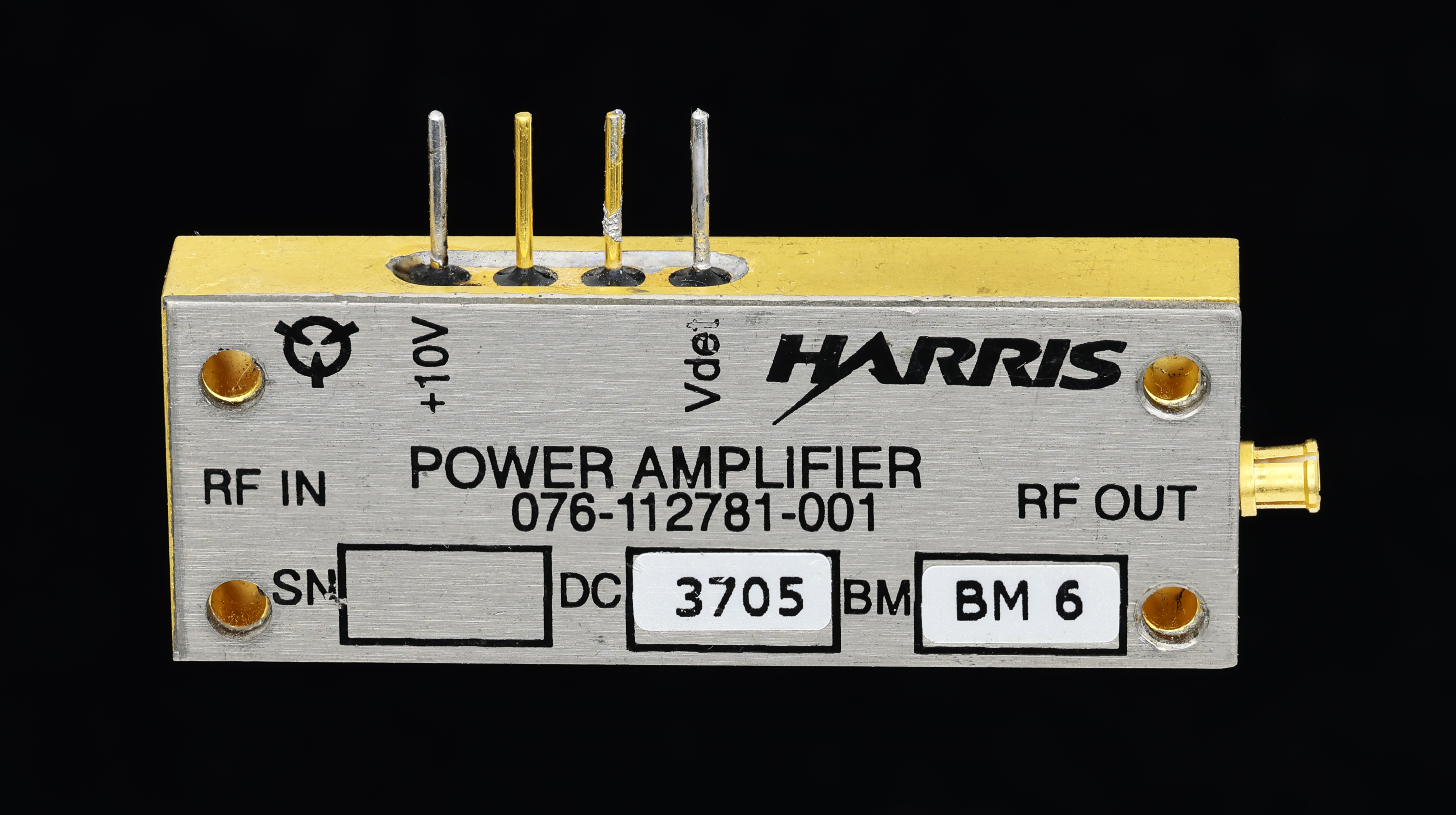
An RF amplifier module shows radio frequency (RF) input and output ports and, separately, direct current (DC) power pins, sometimes beside enable lines, bias settings, or monitor outputs. Bias is the DC level that holds a transistor at its intended operating point. Analog and power ICs, short for integrated circuits, serve those power and control connections, and different IC classes suit different jobs. This article helps RF module engineers and analog IC designers decide which IC class fits each function before choosing a part number.
Five more terms recur below. A power amplifier (PA) raises the level of the RF carrier, the signal that carries the information. An operational amplifier (op amp) is a general-purpose amplifier IC, usually wrapped in feedback to condition or compare signals. A supply rail is a connection that provides power at a particular voltage; it can be regulated or unregulated. Sequencing is the order and timing in which power and bias are applied and removed. A power-management integrated circuit (PMIC) combines functions such as regulation and sequencing; how many rails it makes depends on the part.
Key takeaways
- Carrier gain, control feedback, bias, switching drive, supply rails, and monitoring are separate jobs that are often served by different IC classes, though some can be integrated.
- Op amps usually condition control signals beside the RF stage; they do not replace the RF PA.
- Rail voltage, noise, and power-up order come from the load’s datasheet, not from a universal recipe.
One RF module, several electrical jobs
Around the PA sit five other jobs: setting gain, holding the transistor at its operating point, switching power where a pulsed supply is used, creating supply rails, and watching for faults. Each has different speed, voltage, and noise needs, so one IC class rarely covers all of them.
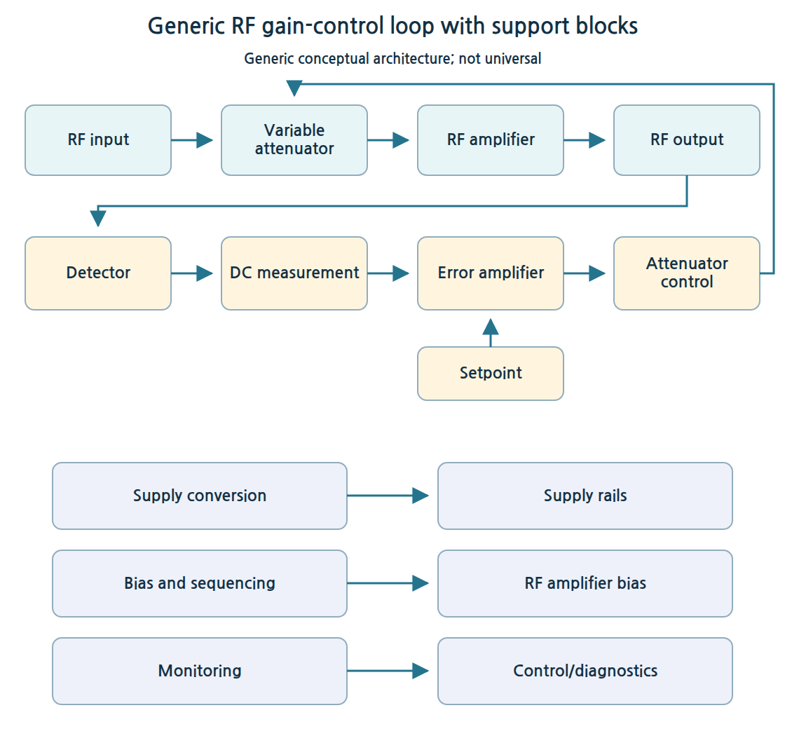
Gain setting often uses a small control loop. An attenuator reduces RF level by a controlled amount. A detector converts RF level into a measurable voltage. The setpoint is the desired target level. An error amplifier compares the target with the measurement and produces the correction.
Figure 1 shows a generic arrangement; the support blocks supply, bias, and watch the amplifier from the side.
Where op amps help, and where they do not
Automatic gain control (AGC) holds output level steady by measuring it and adjusting gain. Analog Devices (ADI) describes a 20 to 37.5 gigahertz (GHz) AGC in its CN0390 circuit note; one GHz is one billion cycles per second. It pairs an RF detector, a voltage-variable attenuator, and an RF amplifier with an op amp that accumulates the error over time to drive the attenuator. The op amp sees only detector and setpoint voltages; the microwave carrier does not pass through it. ADI says its output range must be able to drive the attenuator, and the original circuit uses plus and minus 5 volt supplies. This is an illustrative example, not a product recommendation.
ADI’s AN-2578 application note shows a similar pattern in a temperature-compensated on-chip RF detector: an op amp subtracts the detector voltage from a reference voltage, giving an output that is temperature-stable and proportional to RF power level. Neither example establishes a need for a high-voltage or high-output-power op amp; that depends on the load the control signal drives.
Op amps are not confined to slow signals. Texas Instruments (TI) publishes a tutorial on high-speed op amps in RF applications, so a broadband op amp can suit signals within an appropriate bandwidth and impedance range. The categories still differ: a precision op amp favors low offset, a power op amp favors output current, and an RF PA delivers carrier power.
Bias control and gate drive are different jobs
Bias control sets the transistor’s operating point, often by adjusting gate voltage until drain current reaches a target. Sequencing then matters at power-up and power-down, and the order comes from the transistor’s datasheet; there is no universal sequence.
ADI describes its HMC920 active bias controller as generating a regulated drain voltage and adjusting an external amplifier’s gate voltage to hold a constant bias current, with automated power-up sequencing. The public page describes enhancement and depletion type amplifiers operating in Class-A regime, meaning the amplifying transistor conducts throughout the RF signal cycle, with drain voltages from 3 to 15 volts and drain currents up to 500 milliamps. That is the published envelope, subject to all datasheet operating conditions, and not every combination of specifications is guaranteed, so it is an example of Class-A operation, not of arbitrary high-power supplies. It also lists short-circuit power foldback, which reduces power during a fault, and adjustable current alarms. An alarm reports a condition; shutting the system down remains a system decision, and datasheet conditions apply.
A gate driver is a different part: an IC that quickly charges and discharges the control terminal of a power switching transistor, a role that exists only when an external switching power stage is present. TI’s TIDA-010289 reference design pairs a bias controller with a power stage of two switches between supply and ground, supporting gate or drain pulsing, current monitoring, and power sequencing.
Power management starts with the rail
Power management starts with what the rail must feed: voltage, current, transient response (how it holds up when the load changes suddenly), noise spectrum, headroom, and heat. Headroom is how far the input voltage sits above the output voltage. No single regulator fits every rail.
TI classifies the LP87702 as a PMIC for industrial radar, with two step-down converters, one 5 volt step-up converter, and diagnostic functions. It is a bounded example of low-voltage rails for radar electronic circuits, not a supply for arbitrary high-power RF drain rails.
A low-dropout regulator (LDO) is a linear regulator that works with a small input-to-output voltage difference; the heat it dissipates is about that difference multiplied by the load current. ADI describes how switching supplies leave ripple and ringing: ripple is a small periodic voltage variation at the output, and ringing is a decaying oscillation after fast switching edges. Either can disturb noise-sensitive RF circuits. An LDO after the switcher can help, but its supply rejection, meaning how well it keeps input-supply disturbances from appearing at its output, depends on frequency, load current, and headroom, and more headroom costs efficiency. Noise sensitivity does not automatically mandate an LDO.
A counterexample matters. In an ADI case study, one selected 5 volt rail of a frequency-generation circuit is powered by an ultralow-noise switching regulator while its 3.3 volt rail stays on an LDO. ADI reports application-specific spectral trade-offs, so conditions matter. Check the noise spectrum against the load’s sensitivity and weigh the losses before adding a stage.
A practical function-to-IC checklist
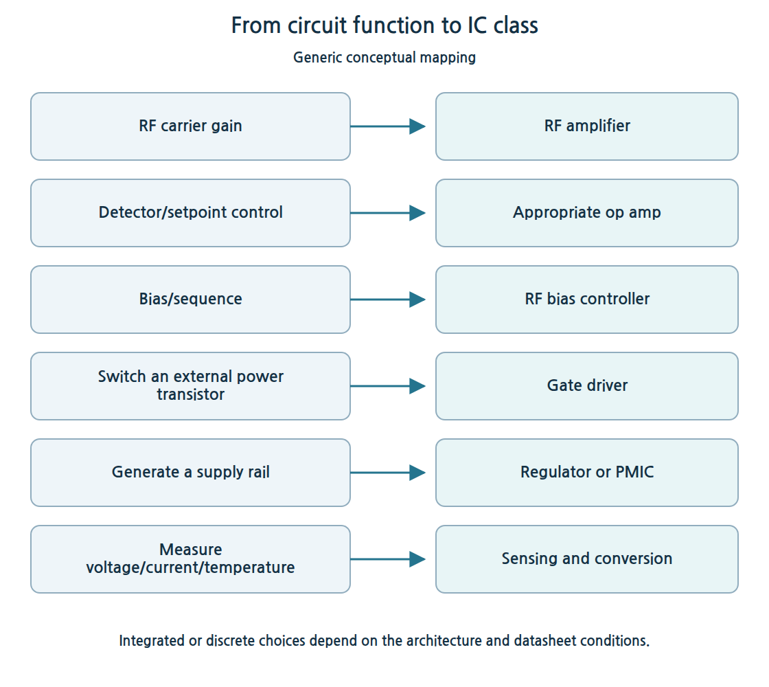
A digital-to-analog converter (DAC) turns a digital code into a voltage, for example to set a target level. An analog-to-digital converter (ADC) turns a voltage into a digital code, for example to read a monitor signal. Figure 2 maps functions to IC classes, not parts; the table adds one measurement and one fault question for each. Measure within the module’s rated limits and the datasheet’s test setup.
| Function | Typical IC class | Measurement and fault question |
|---|---|---|
| RF carrier gain | RF amplifier | Measure gain and output level across the control range. What does the output do if the control input is lost? |
| Detector/setpoint control | Appropriate op amp; DAC setpoint | Plot detector voltage against RF level. Does the loop settle without oscillating when the setpoint steps? |
| Bias/sequence | RF bias controller | Measure drain current against bias setting over temperature. Does the power-up and power-down order match the datasheet? |
| Switch an external power transistor | Gate driver | Capture the gate waveform under load. What happens if the drive signal stalls? |
| Generate a supply rail | Regulator or PMIC | Measure ripple and noise at the load pin during a load step. Does the rail stay within limits when the input droops? |
| Measure voltage/current/temperature | Sensing and conversion; ADC reading | Compare ADC readings with a reference instrument. What does the system do, and how fast, if a rail droops or bias drifts? |
Whether these functions share one IC or several depends on architecture, voltage, and board space.
Next step, sources, and credits
Take your module’s block diagram, write the six rows with the real load requirements, and mark each row whose answer depends on a datasheet you have not yet read. Related reading: RF module package choices and analog IC production hand-off.
Selected primary sources (publisher statements are attributed; examples are illustrative and some are older foundational material, not recommendations or current capability claims):
- ADI, CN0390 circuit note: an op amp as AGC loop controller
- ADI, AN-2578 application note: detector and reference subtraction
- TI, TIDA-010289 reference design: bias controller with gate or drain pulsing
- ADI, HMC920 product page: bias controller class and listed limits
- TI, LP87702 product page: low-voltage radar PMIC classification
- ADI, LDO headroom article: switching noise and LDO trade-offs
- ADI, ultralow-noise switcher article: one-rail counterexample
- TI, op amps in RF applications tutorial (1993, revised 2013): high-speed op amps
Photo credit: RF amplifier module, Wikimedia Commons file page, by Mister rf, 18 May 2026, licensed CC BY-SA 4.0. Displayed at a responsive size; original full frame. Manufacture date unknown; no affiliation or endorsement is implied, and the photograph is not used to identify internal parts.
The third-party photograph keeps its linked CC BY-SA license, and the notice below concerns the article text only; it adds no image-use restrictions.
Please link to this article when sharing. Contact us for permission to republish the full article.