
Intel Foundry test and die-sort equipment in a cleanroom facility. Capture date not provided. Photo: © Intel Corporation (source).
Before an analog IC moves from one test provider to the next, someone has to decide which stage measures what, at which temperature, against which limits, and who may release the result. Writing those decisions down makes the next handoff easier to evaluate. This article describes how to plan an analog IC production handoff before material ships.
It is written for design, product and operations teams working with a foundry, a wafer-test provider, an assembly and final-test provider, and a customer quality owner. The checklist below is our own proposed practical framework, not an industry standard, and every item must be adapted to the product.
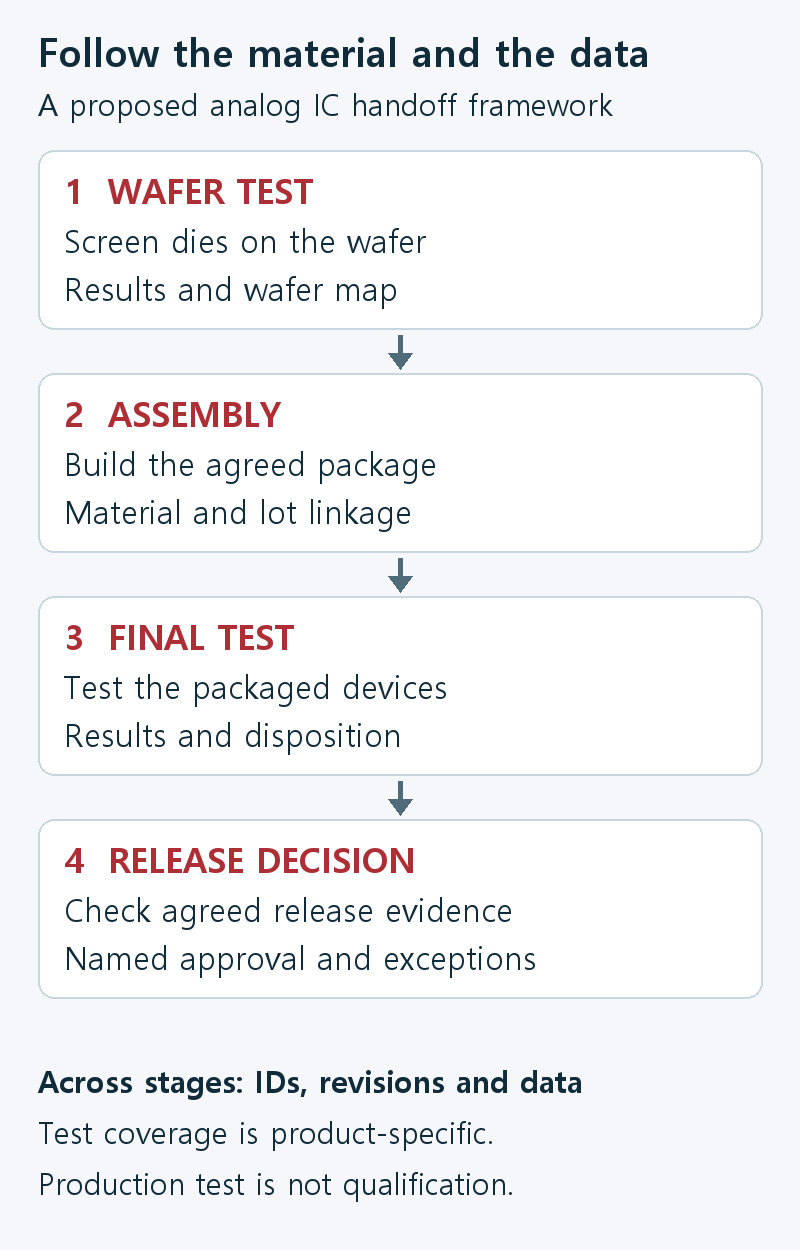
Wafer test, assembly and final test do different jobs
In the conventional flow, Texas Instruments describes wafer probing as an electrical check of individual die before packaging, assembly as the die attach, interconnect and molding steps, and final test as a check of the packaged device. Advanced packages may follow a different sequence.
The stages differ because the device differs. A die on a wafer has not yet seen the thermal and mechanical effects of packaging. A packaged part is measured on different hardware, with different contacts and a different handling path. A pass at one stage is therefore evidence for that stage only.
Packaging can change precision parameters. A TI application note on offset correction explains that physical stress after singulation and packaging can shift an amplifier’s input offset, and describes both wafer-level laser trim and a package-level trim implementation. This amplifier example makes trim timing a useful design question: which package-related shifts can the chosen trim method correct?
Screening, characterization and qualification are separate
Routine production testing screens individual units against the agreed specification. Characterization explores how a design behaves across process, voltage and temperature. Qualification uses stress to judge reliability. TI’s quality overview separates development testing across manufacturing, voltage and temperature extremes, qualification using accelerated stress, and production verification that is parametric, functional and visual.
Analog Devices likewise describes qualification that considers the intended application and environment, accelerated stresses that assess robustness, and ongoing monitoring of sampled production units.
The practical consequence is that characterization and qualification evidence should inform what production tests are needed. The coverage plan should state which specifications are measured on each unit and which rely on sampling, characterization or design evidence. Production electrical tests do not replace reliability qualification. For process-level background, see our earlier note on choosing between SOI and BCD for high-voltage analog.
Make wafer maps and traceability usable by the receiver
Handing over results means handing over context. The SEMI E142 specification for substrate mapping addresses how map data for wafers, frames, strips and trays is stored, reported and transmitted, including through assembly, packaging and test. A SEMI article on supply-chain traceability explains that the E142 data model can help associate assembly components with process and material history, so upstream and downstream assets can be linked. The recommendations below use that general mapping purpose; implementing E142 requires the applicable specification.
In practice, ask the sender to specify and the receiver to confirm wafer identity, map orientation and coordinates, the meaning of each bin, the approved map revision, and reconciliation of material counts. Agree how far traceability goes. Linking wafer or lot identity, die location where supported, assembly lots, test results and shipment identifiers is useful, but do not assume every package is individually serialized unless that has been implemented and verified.
Check correlation and control retest
Correlation means checking that comparable measurements agree under defined conditions, within a relationship the team has agreed. It does not mean every wafer result equals every final result. When values shift, investigate the product, packaging and measurement setup, including contacts and test conditions.
Retest needs equally clear rules. Our suggestion is to define in advance which failures are eligible, who may approve a retest, the allowed sequence and count, which records are retained, and how initial and retest results affect disposition. Avoid repeated testing merely to obtain a pass, or limit changes made solely to raise yield. Yield is a useful signal, but it should not be the sole release criterion.
A proposed handoff checklist
Use these six checks before transfer. Agree the suggested responsibilities with the parties involved.
1. Agree what each stage tests
Evidence: A test-allocation document covering wafer test, final electrical test, temperature and voltage coverage, and which conditions are verified by other means.
Owner and decision: Product or test engineering proposes; the design owner and customer quality owner approve.
2. Fix limits, trim stage and revisions
Evidence: Controlled limits, guardbands, trim stage, and test program and hardware revisions.
Owner and decision: Test engineering owns the files; the design owner decides on limit changes; quality records approval.
3. Confirm map and identity
Evidence: Receipt confirmation of wafer ID, map orientation, bin definitions, approved map revision and counts.
Owner and decision: The receiving operations lead confirms; any mismatch goes to a defined hold.
4. Set correlation checks
Evidence: Agreed comparable measurements, conditions and acceptable relationships, with review of any shift.
Owner and decision: Test engineering reviews; the product owner decides whether a shift is acceptable or needs investigation.
5. Control retest and nonconformance
Evidence: A retest procedure, original and retest records, and the disposition for each abnormal result.
Owner and decision: Quality owns disposition. Define responses separately for a failed unit, an unusual lot/bin pattern and a suspected test-setup fault.
6. Make the release decision
Evidence: Yield and bin summary, unexplained-shift review, open nonconformances, traceability links at the agreed granularity, and the relevant qualification evidence.
Owner and decision: The named product, test and quality decision makers sign off together; yield alone does not release material.
Confirm the site behind a supplier’s service list
For teams evaluating production in China, a practical first step is to separate group-wide services from evidence for the intended plant. JCET’s Test Solutions page describes wafer-probe and final-test services, while its Worldwide Locations page identifies named entities and addresses in China and other countries. Use the service list and location information to prepare questions for the named site, then obtain current product-specific evidence.
For any project, in China or elsewhere, confirm the named legal entity and physical site, the test platform and its voltage and temperature capability, the package flow, the data interface, and the change-control and disposition contacts. Confirm that the qualification evidence covers the intended product, process, package and site. If a design is being moved, our note on what must be reproven when porting a power analog process covers the design side.
A handoff is ready when each stage can say what it tested, under which conditions, with which revisions, and who will decide when something looks wrong.
Photo credit
Featured photo: Intel Foundry test and die-sort equipment in a cleanroom facility; capture date not provided. © Intel Corporation, used as an editorial (news and article) image under the Intel Press Hub media-asset terms. Source: Intel Foundry Direct Connect 2025 press kit. The inline handoff diagram is an original ChinaSemiOps illustration of a simplified wafer-test, assembly and final-test sequence; it does not depict a specific facility or equipment model.
Selected primary sources
- TI: Assembly & test – wafer probe, assembly and final test descriptions.
- TI SBOT037D: Offset Correction Methods – package stress and trim examples; revision D, December 2024.
- TI: Quality – development, qualification and production testing.
- Analog Devices: Reliability – qualification and ongoing monitoring.
- SEMI E142-0225 abstract – substrate map data exchange.
- SEMI: Traceability and Security across the Supply Chain – linking material and assembly history.
- JCET: Test Solutions – provider-described wafer-probe and final-test services.
- JCET: Worldwide Locations – named entities and site addresses.
Please link to this article when sharing. Contact us for permission to republish the full article.