Choosing a DrMOS power stage is not mainly a choice between ampere labels. Integration can shrink the switching cell, reduce internal parasitics and place gate-drive timing, MOSFETs and sometimes sensing inside one package. It does not complete the voltage regulator.
The decision is whether integration improves power density at the intended operating point. The controller, passives, printed circuit board (PCB), cooling and protection still have to work as one system.
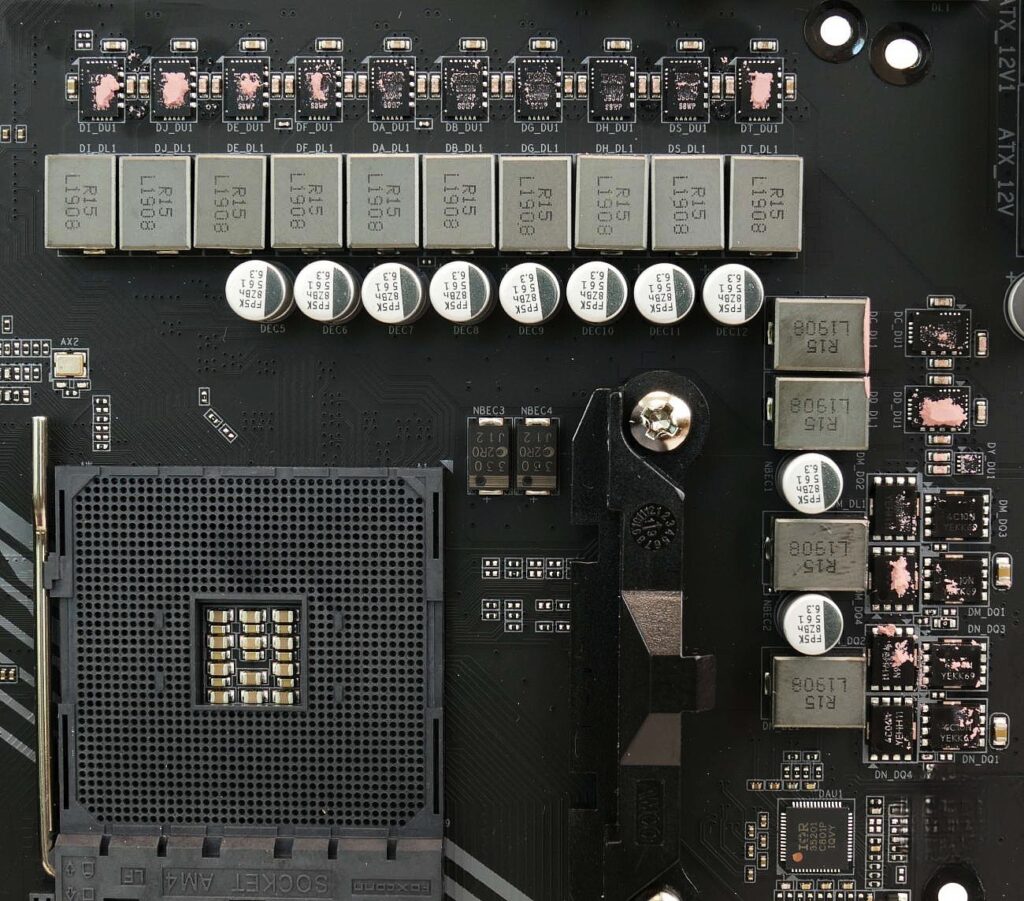
Featured photograph: a modern motherboard voltage-regulator module. StefanEnDev via Wikimedia Commons, CC0 1.0. Used as an illustration of a multiphase VRM layout; the source does not identify the individual power-stage parts.
Three takeaways
- DrMOS integrates the driver and two power MOSFETs; the control loop and energy-storage components usually remain outside.
- Current ratings are filters, not normalized performance comparisons. Loss and temperature at the intended operating point matter more.
- A successful selection closes four contracts together: electrical interface, switching behavior, telemetry/protection and the board thermal path.
What DrMOS puts inside the package
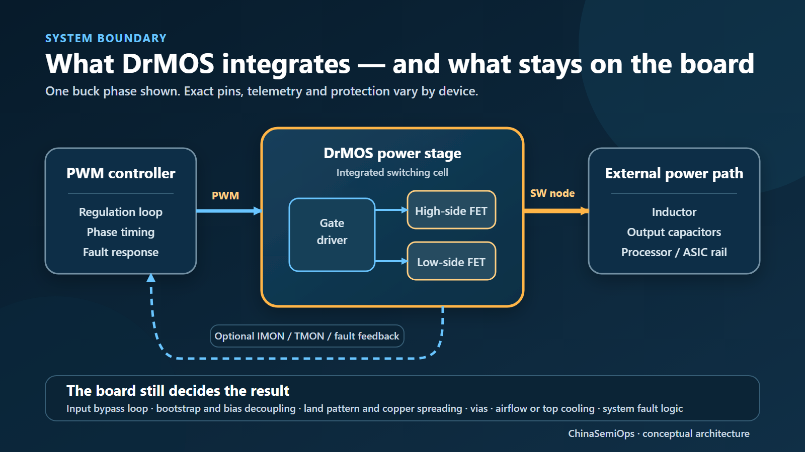
DrMOS is short for driver-MOSFET. The package contains the gate driver and two MOSFETs for one buck phase. An external pulse-width modulation (PWM) or multiphase controller regulates the output; the inductor and capacitors remain external.
Short internal connections can reduce parasitics compared with a driver and two discrete MOSFET packages. The integrated driver also controls dead time: too little risks shoot-through, while too much increases body-diode conduction.
Modern products extend this boundary differently. “Smart power stage,” “SPS” and similar terms may add sensing, fault flags, protection or bootstrap refresh; the names do not define one universal feature set.
Treat PWM compatibility as a threshold-and-timing contract, not a “3.3 V” or “5 V” label. Logic windows, tri-state behavior and hold-off timing can differ by device and suffix.
Confirmed architecture: the onsemi NCP303150 datasheet shows an external controller, inductor and capacitors around the integrated switching stage.
Where integrated stages fit
The recurring application is a low-voltage, high-current multiphase rail. Vendors document stages for processors, GPUs, memory, field-programmable gate arrays (FPGAs), AI accelerators and network ASICs.
The cited design and deployment examples are engineering evidence, not a current-product inventory. TI reference design TIDA-010241 uses CSD95410 stages for Intel and Xilinx FPGA platforms. Renesas publishes an AI-accelerator architecture for high-current, sub-1 V rails. Infineon states that Supermicro MicroBlade servers use TDA21490 and TDA21535 stages. They show how integrated stages have been applied; they do not identify the newest devices or establish present availability.
These are different evidence levels: reference design, reference architecture and vendor/customer deployment statement. None is an independent cross-vendor benchmark.
What the current market adds
Checked 15 September 2026: recent official material documents compact single-phase stages and one new dual-phase design. The MPS MP87000-M datasheet, Rev. 1.0, 22 April 2025 describes a 5 × 6 mm DrMOS with up to 90 A continuous output current plus current and temperature reporting. AOS labels the AOZ52986QI New and specifies a 3 × 4 mm SPS with 45 A continuous current, current and temperature outputs, and a product brief dated 8 May 2026. Its pulse-current statements depend on input voltage and pulse duration.
Infineon introduced the dual-phase TDA235E5 and TDA235E0 on 7 September 2026. Infineon states 120 A total design current and up to 300 A peak current in a 6 × 6 × 0.8 mm³ package. Engineering samples are currently available for customer evaluation; the announcement does not state production availability.
This snapshot records vendor-stated capabilities and lifecycle positions on the check date. It is not a shortlist, recommendation or normalized comparison. The same interface, loss, telemetry, protection and thermal checks still apply.
Why the ampere label cannot make the decision
Current labels include peak, average, continuous and timed pulse ratings, with different switching and thermal conditions.
The following older datasheets are retained because they expose useful rating definitions and test conditions. Their inclusion is not a claim of current availability or product preference.
The TDA21490 datasheet’s absolute-maximum table lists 90 A peak and 70 A maximum average. Renesas says ISL99390 supports 90 A DC but does not publish a complete board and airflow condition in its short-form sheet. These are vendor-stated limits under each document’s definitions, not a normalized comparison.
The onsemi NCP303150 datasheet shows why conditions matter: its board-dependent average-current example gives 50 A at 19 V input, 1.0 V output, 300 kHz and 25 °C ambient, then 45 A when frequency rises to 1 MHz. Higher frequency can improve transient response and reduce passive size while increasing switching loss.
Engineering inference: compare power loss and steady-state temperature at your VIN, VOUT, frequency and phase current before comparing headline current. Repeat at the hot corner and during realistic load steps. A current number without that context is an initial filter.
Use four contracts to screen a candidate
The table below is an original decision aid for moving from a parametric search to a board-ready shortlist.
| Contract to close | Check before schematic release | Prove on the board |
|---|---|---|
| Electrical interface | Exact suffix; PWM high, low and tri-state windows; bias rails; enable polarity; startup sequence; controller compatibility | Clean state transitions during startup, reset, light-load mode and shutdown; no unintended turn-on |
| Switching behavior | VIN/VOUT range; frequency; minimum pulse width; propagation delay; bootstrap capacitor and refresh behavior | Switch-node overshoot/undershoot, ringing, dead-time behavior and transient response over line/load/temperature |
| Telemetry and protection | Current-sense gain, offset, bandwidth and valid range; temperature output versus warning flag; overcurrent/thermal fault action | Per-phase current accuracy and balance; calibration; short, overcurrent and overtemperature response; controller reaction to every fault |
| Thermal and physical path | Exact land pattern and pinout; package height; exposed pads; junction-to-board/top thermal metrics; vendor PCB assumptions | Hottest junction, nearby inductor heating, copper/via spreading, airflow or top cooling, and sustained workload margin |
Telemetry deserves careful treatment. The Renesas ISL99390 sheet states ±3% continuous current monitoring and an 8 mV/°C temperature output. The MPS MP86957 sheet specifies sense accuracy over a defined current range. The AOS AOZ5311NQI sheet instead provides a thermal-warning output and assigns system current protection to the controller.
That difference changes controller choice, calibration and fault testing. “Integrated current sense” is incomplete unless gain, reference, blanking and valid range match the controller. A thermal-warning flag is not continuous temperature telemetry.
Integration does not make layout forgiving
The external high-di/dt loop still runs through the local input capacitor, switches and ground return. Keep it short: place ceramic input capacitors across VIN and power ground, keep bootstrap and bias decoupling close, and route sense pairs away from the switch node.
A junction-to-ambient value measured on a vendor test board cannot predict a dense product board. Copper, vias, airflow, adjacent phases and inductor heating change the result. Even “common” 5 × 6 mm packages may differ in pinout, exposed pads and land pattern.
Open qualification question: where is the hottest semiconductor junction during the sustained workload and the worst load transient? Answer it with measured loss and temperature on the intended board, not a package outline or room-temperature efficiency curve.
The practical next action
Freeze one operating-point sheet before selection: VIN/VOUT, switching frequency, sustained and transient phase current, cooling boundary, controller and PWM levels, telemetry accuracy, and required fault response.
Compare every candidate against that sheet. Validate startup, load steps, sensing, faults, switch-node stress and thermal steady state on hardware. DrMOS earns its place when integration improves density and repeatability while those margins still close.
For the surrounding power path, read 48 V to the AI Core: Where the Conversion Boundary Becomes the IC Problem, Inside the 48 V AI-Server eFuse, and Co-Packaged Optics and Its IC Supply Chain.
Disclosure: Products are public engineering examples, not endorsements or evidence of a commercial relationship. Specifications are vendor-stated under their cited conditions. This article is an engineering selection framework, not a product qualification.
Selected primary sources
- Infineon TDA21490 datasheet, Rev. 2.0, 1 December 2020 — envelope, telemetry, protection and thermal data.
- Renesas ISL99390R5935 / BR5935 short-form datasheet, Rev. 1.01, 1 December 2023 — PWM variants and sensing.
- MPS MP86957 datasheet, Rev. 1.1, 10 July 2020 — sensing, protection and thermal metrics.
- onsemi NCP303150 datasheet, Rev. 3, July 2022 — conditioned current ratings and layout.
- AOS AOZ5311NQI datasheet, Rev. 1.2, April 2021 — thermal warning and system boundary.
- TI TIDA-010241 reference design, September 2022 — FPGA multiphase implementation.
- Renesas AI accelerator power architecture — sub-1 V accelerator context.
- MPS MP87000-M datasheet, Rev. 1.0, 22 April 2025 — recent stage with up to 90 A continuous output current plus current and temperature reporting.
- AOS AOZ52986QI product page and 8 May 2026 product brief — compact new SPS with conditioned continuous and pulse-current statements.
- Infineon TDA235E5/TDA235E0 introduction, 7 September 2026 — emerging dual-phase engineering-sample family.