One Isolation Barrier, Four Different Gate-Drive Problems
Added an isolation-ratings comparison and a worked datasheet example.
Engineering analysis and practical perspectives on semiconductor design, manufacturing and supply chains.
42 / 42
Added an isolation-ratings comparison and a worked datasheet example.
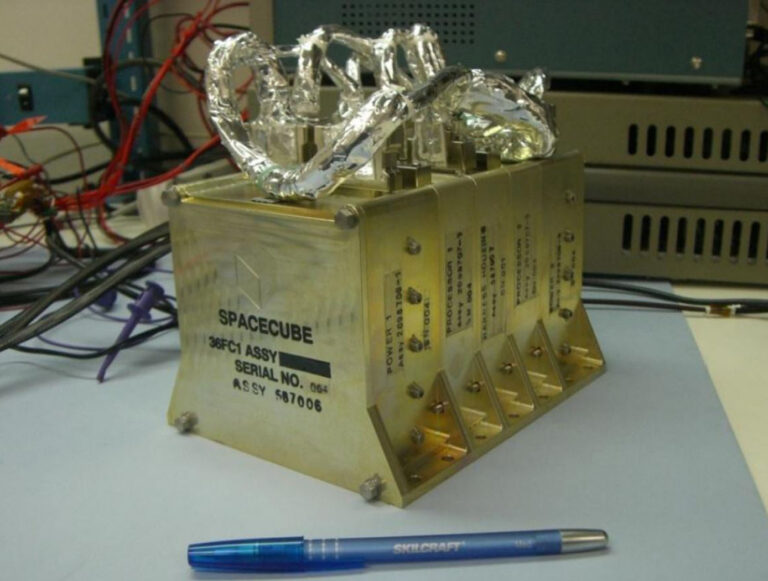
Updated the technical analysis and application photograph.
Topic labels and reading paths are editorial reading aids.
A 200 mm SiC wafer has about 1.78 times the area of a 150 mm wafer, but buyers pay for accepted devices. Learn how to compare cost per accepted die and what evidence to ask suppliers for.
Read More →Manufacturing, packaging & test · China ecosystem & qualification
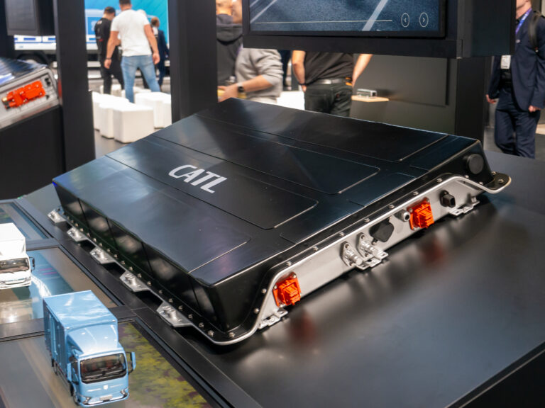
How an EV traction pack connects safely to its inverter and lets go when something fails: precharge, contactors, fuses, pyro disconnects, drivers and the energy that remains afterwards.
Read More →Power electronics & applications
A hypothetical failed converter shows why SiC and GaN failure analysis should start with preserved evidence, a method matched to the question, and an agreed hold point before any irreversible step, such as opening the package or cutting.
Read More →Manufacturing, packaging & test
A current-sense output spikes at a motor inverter switching edge. Learn when a reading can be trusted and which evidence to request.
Read More →Power electronics & applications · Analog & IC design
A practical qualification workflow for alternative analog ICs: compare test conditions, validate the signal chain and record an application-specific release.
Read More →Analog & IC design · China ecosystem & qualification
A battery-storage inverter design decision, and why a peak-efficiency headline is only the start: what hybrid SiC modules contain, where efficiency boundaries sit, and which evidence to request from suppliers.
Read More →Power electronics & applications
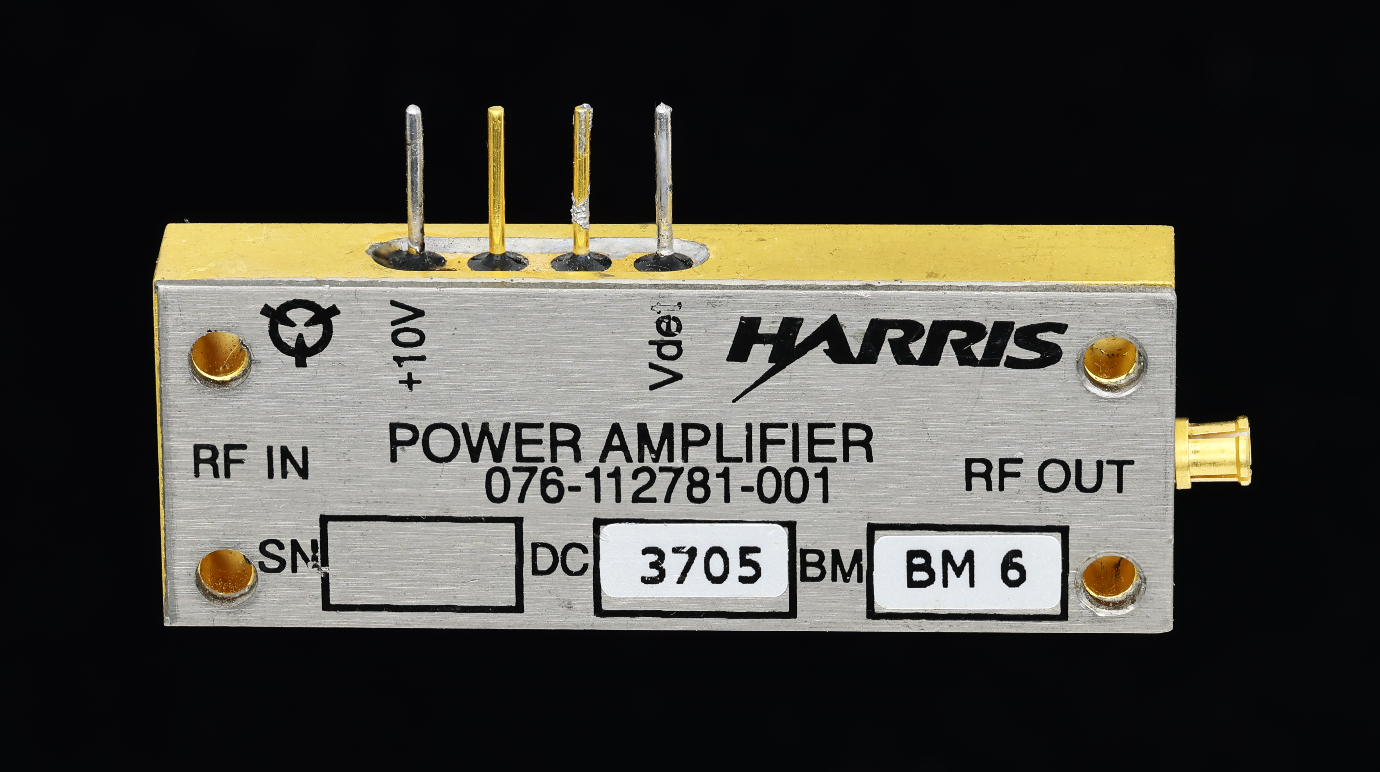
An RF amplifier module shows RF ports and separate power pins. This article maps six circuit functions to the analog and power IC classes that usually serve them, with one measurement and one fault question for each.
Read More →Power electronics & applications · Analog & IC design
HTCC vs LTCC selection depends on the complete ceramic, conductor and assembly stack. Compare electrical loss, heat flow, sealing and production evidence.
Read More →Manufacturing, packaging & test
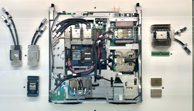
Five processor labels overlap. Start with your AI workload, check software and memory, then map who designs, builds, packages and tests the system.
Read More →Analog & IC design
Start from the RF function, not the package name. This guide compares bare die, QFN and flanged housings, explains GaN bias order and heat path, and lists the evidence to request from a supplier.
Read More →Manufacturing, packaging & test · China ecosystem & qualification
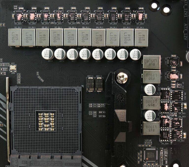
A CPU or GPU VRM is more than its DrMOS power stages. See how controllers, phases, inductors and capacitors work together, why voltage dips when load jumps, and what TLVR changes.
Read More →Power electronics & applications · Analog & IC design
How to plan an analog IC production handoff: what wafer test and final test each cover, why trim stage and package stress matter, and a proposed checklist for evidence, owners and release decisions.
Read More →Manufacturing, packaging & test
A practical guide to radiation-hardened IC selection: connect dose and single-event evidence with analog accuracy, power protection and mission requirements.
Read More →Analog & IC design · Manufacturing, packaging & test
A biosensing analog front end must match the sensor's electrical output: ECG voltage, bioimpedance excitation or electrochemical current. See what vendor specifications do and do not tell you.
Read More →Analog & IC design
How sensing, signal conditioning and actuator feedback help engineers choose analog interfaces and validate fault response in AI-server liquid cooling.
Read More →Power electronics & applications · Analog & IC design
A practical four-part framework for evaluating DrMOS interfaces, switching behavior, telemetry, protection, and board-level thermal performance.
Read More →Power electronics & applications
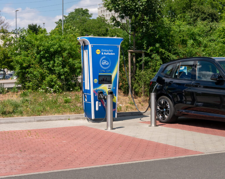
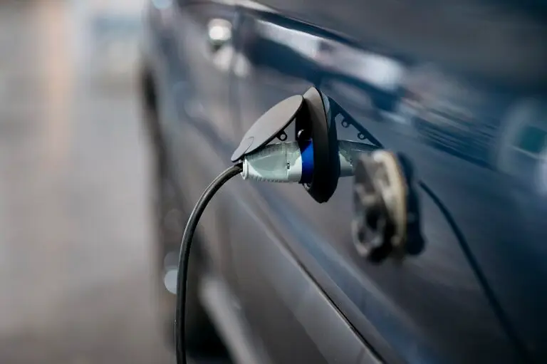
Megawatt charging safety depends on more than a larger connector. This architecture guide maps which sensing, insulation, thermal and shutdown functions may merit integration—and which should remain external.
Read More →Power electronics & applications
EV onboard charger technology is advancing through bidirectional architectures, SiC/GaN switching, control, isolation and thermal co-design. Here is the engineering decision map.
Read More →Power electronics & applications
Inverter control ICs sit around the switch bridge. Use this function map to screen sensing, gate drive, protection, bias and telemetry opportunities by application.
Read More →Power electronics & applications · Analog & IC design
48V AI rack power is becoming a conversion-boundary decision: retain an intermediate bus, move a high-ratio stage close to the accelerator, or use package-adjacent delivery. This public-source analysis maps the IC, PDN, thermal and service trade-offs.
Read More →Power electronics & applications
Isolation ratings answer different questions. A table of what each rating is for and one dated datasheet reading, set against the different gate-drive needs of IGBT, SiC, superjunction MOSFET and GaN stages.
Read More →Power electronics & applications · Analog & IC design
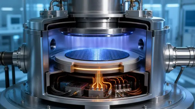
An electrostatic chuck supply is more than a kilovolt source. Clamp and release waveforms, low-current sensing, RF coexistence, fault handling, and the boundary between custom ICs and external high-voltage hardware shape the real architecture decision.
Read More →Power electronics & applications · Analog & IC design
Piezo haptics, nanopositioning, ultrasonic cleaning, inkjet and medical ultrasound may all need high-voltage drive, but they require very different IC architectures. This practical map shows where each approach fits and where analog IC opportunities remain.
Read More →Power electronics & applications · Analog & IC design
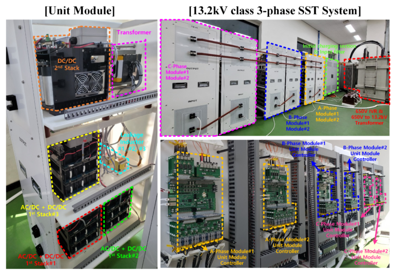
Solid-state transformers create real semiconductor demand, but not for one monolithic transformer chip. This evidence-led architecture map shows where SiC modules, isolated gate drivers, sensing, bias power, protection and control actually fit—and what must be proven before calling any function a custom-IC opportunity.
Read More →Power electronics & applications
HVAC growth creates its strongest semiconductor openings in inverter gate drivers, PFC, motor control, sensing and protection. This load-first map separates repeatable platforms from specialized, safety-heavy functions.
Read More →Power electronics & applications
The planned Navitas–Magnachip SiC transfer highlights a broader rule: masks and recipes may move, but manufacturing behavior, models, reliability, test and route-release evidence must be re-established.
Read More →Manufacturing, packaging & test · China ecosystem & qualification
See where copper still wins, where fiber takes over, and how pluggable optics, LPO, CPO and optical I/O shift system responsibility.
Read More →Analog & IC design
At a 48/54 V AI-server input, protection must do more than limit inrush. Integrated eFuses and external-MOSFET hot-swap controllers make different tradeoffs in safe operating area, current scaling, thermal design, fault timing and telemetry. Here is how to compare them on equal terms.
Read More →Power electronics & applications
The low-altitude economy extends far beyond passenger eVTOL. Industrial UAVs, cargo aircraft, docks, chargers, protected power distribution and diagnostic telemetry may create earlier opportunities for power-analog IC suppliers.
Read More →Power electronics & applications
At multi-kilovolt, hundreds-of-amp scale, device speed is only part of the contest. DC fault energy, always-on breaker losses, microsecond protection windows, hybrid architectures, packaging, and qualification increasingly decide which power-semiconductor systems are viable.
Read More →Power electronics & applications
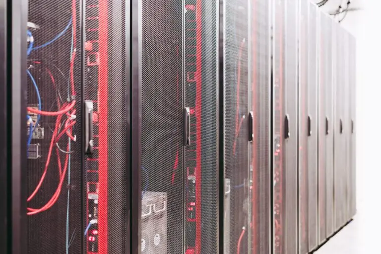
800 VDC receives attention for GaN and SiC conversion, but the less-visible design frontier is the analog protection boundary that must connect, measure, diagnose, and isolate high-power compute trays.
Read More →Power electronics & applications
The useful question is not which process is better. It is whether isolation, thermal path, power-device integration, reliability, package, and test assumptions match the product risk.
Read More →Analog & IC design · Manufacturing, packaging & test
AI infrastructure is not only a GPU story. Rising rack power, fast load transients, 48 V rack limits, and emerging 800 VDC architectures are moving hard problems back into analog and power IC design. The opportunity is real, but it must be framed as a source-backed design-space opening, not a guaranteed socket.
Read More →Power electronics & applications
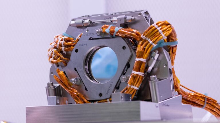
ADI's 32-channel HV DAC driver family is in lifecycle transition. Here is what the drive current and settling delta means for OCS MEMS mirror designs - and what you need to validate.
Read More →Analog & IC design
Graphene is one of the most over-cited materials in semiconductor presentations. Most commercial "graphene" products are reduced graphene oxide or pyrolytic graphite, not monolayer CVD graphene. Two applications have crossed into commercial production. Everything else — including BEOL interconnects and logic transistors — is laboratory research. This insight separates the genuine near-term opportunities from the decade-long research bets.
Read More →Manufacturing, packaging & test · China ecosystem & qualification
High voltage alone does not force a ceramic package. Ceramic becomes compelling when voltage combines with high current, power dissipation, hermeticity, harsh environments, or long-life reliability requirements. The real growth is in EV power electronics, renewable inverters, AI data-center power, industrial drives, RF, aerospace, and medical high-voltage systems.
Read More →Manufacturing, packaging & test
Co-packaged optics is shipping at the leading edge — Broadcom's Bailly platform is customer-delivered — but the next switch generation and most published "CPO market size" figures are still a roadmap slide, not a 2026 reality. This insight separates what is actually deployed from what is announced, and shows where the AI-server and CPO power management opportunities genuinely differ in evidence and maturity.
Read More →Analog & IC design
NVIDIA publicly names Navitas in its 800 VDC AI data center power ecosystem, and Navitas has demonstrated relevant GaN power hardware. But the public record does not yet prove a disclosed production socket inside an NVIDIA AI server package. The difference matters for power semiconductor strategy.
Read More →Power electronics & applications · China ecosystem & qualification
TI TIDA-010979 and EPC23102 already validate the humanoid joint GaN thesis — and claim the reference platform position. A generic gate driver or GaN power stage competes head-on with both. The real opening is a companion IC for current sensing, safe-disable, and regen coordination.
Read More →Power electronics & applications · Analog & IC design
The 3D printing market is growing, but the real power analog IC opportunity depends on printer architecture, printhead control, and who owns the waveform socket.
Read More →Power electronics & applications · Analog & IC design
A factual guide to the universal pricing logic used by semiconductor foundries. This post decodes the industry-standard cost structures for MPW (grid-based seat allocation) and Full-Mask NTO (layer-proportional NRE), providing the essential formulas for PMs and engineers before requesting a quote
Read More →Manufacturing, packaging & test · China ecosystem & qualification
Global standards like WAT and SBL exist everywhere, but in China, they operate under different pressures: speed, scale, and localization. Here is how to align your engineering expectations with the reality of Chinese mass production.
Read More →Manufacturing, packaging & test · China ecosystem & qualification
No Insights match your search.